I am starting this thread to present my latest amp design using Hitachi lateral FETs. This is a remake of my designs in the early 80s and born by a rare chance: Earlier this year an old friend of mine gave me a convolute of NOS 2SK135/2SJ50. This was the preferred technique in these days so I decided to do an update. Nowadays I design class-D amps with TI chips being much smarter in size and power consumption with impressive performance. So why re-vitalize this obsolete stuff?
Because there are applications where class-D sucks. And I am not talking about driving loudspeakers in Hi-Fi setups, this is a job they do fairly well. But measuring applications in a lab can be quite annoying with class-D output. For instance look at a small signal of let us say 1Vpp with an oscilloscope - you will not find it hidden in the switching residual.
Another point is full bridged output is not desirable in lab measurements, so the tradiditional split supplied half bridge topology is preferred.
These aspects gave enough excusions for me to fiddle around with another lateral FET amp😉
For those interested in KiCAD I will post my sheets and libs as well, which may be helpful for the beginners. These libs include all my parts used, no need for any other libs.
Attachments
For instance look at a small signal of let us say 1Vpp with an oscilloscope - you will not find it hidden in the switching residual.
It depends on how well the output is filtered and how high the carrier frequency is.
It does, but with practical pwm frequencies of 400~600kHz there is not so much to be gained. And for wider bandwith applications the output filter is a no go.
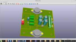
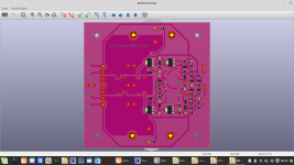
I fiddled about 6 weeks with LTSpice to develop this circuit. The main goals were
-rocket solid design
-power bandwidth >100kHz
-very low THD upto 20kHz ↔ >60dB gain upto several 10kHz
-high CMMR
->40Vpp into 8 Ohms
-asymmetric input, Z>10kOhms
-components available at Mouser (excl latFETs)
Some Circuit Details -The LTP
There is nothing really special here. The current source driven by a voltage reference yields high CMMR.
The VAS
To achieve max speed the cascode configuration is mandatory. Even in cascode configuration BJTs like BD139/140 or MJE340/350 restrict bandwith as well as linearity (early effect). Best results are obtained with fast low voltage types like BC550/BC560 or BC546/556 respectively. For higher supply voltages the derivates of 2N5551/5401 seem to be the next best choice. An active current mirror between differential input pair and VAS provides additional loop gain which is beneficial over the hole frequency range.
Gate Drive Buffer
A complementary emitter follower connects the VAS to the gates of the power MOSFETs. This reduces capacitive loading of the VAS stage and and improves loop stability as well. In the simulations it shows up as a significant improvement of THD specially at higher frequencies.
Slew Rate and Power Bandwidth
These are directly correlated to each other. Here are two bottlenecks that will limit the maximum available voltage slew rate.
1. LTP output charges the miller capacitance. Assume the differential collector current is biased to 2*1mA yielding a max charging current of +/-1mA and a 10pF Miller capacitance. The resulting slewrate is limited to SLR = I/C = e-3/e-11 = e+8 = 100V/us
2. The VAS provides limited current to charge the VAS loading capacitance. Assuming a VAS bias current of 10mA loaded by 100pF this results in
SLR= e-2/e-10 = e+8 = 100V/us
These numbers might give an idea of the practical SLR limits. So aiming at highest slewrate means
- minimize Miller capacitance
- minimize VAS loading capacitance
- maximize VAS bias current
Output Stage
Actually no snubber, no series inductors, no damping resistors. All these things removed that restrict a wideband output. No risk, no fun!
Last edited:
Nice VFA, Voltwide. I like the current mirror.
Just a question, how are-you going to cool the HEXFETS ?
Just a question, how are-you going to cool the HEXFETS ?
This is not so evident, but nonetheless easy to explain. The pcb will be mounted parallell to a heatsink (200*300*20mm) in a short distance of approx 10mm. Each TO-3 will be mounted onto an alu profile 50*100mm, 3~4mm thick. This will be mounted on a massive alu rod (10*10 upto 20*20mm, 100mm long). The resulting heat conductor will be screwed to the aforementioned big heatsink (I have just a pile of them, stored since the eighties)
Last edited:
Btw, there are no HEXFETs, and the hole circuit is not designed for them.Nice VFA, Voltwide. I like the current mirror.
Just a question, how are-you going to cool the HEXFETS ?
The Hitachi MOSFETs, sorry ;-)Btw, there are no HEXFETs, and the hole circuit is not designed for them.
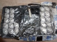
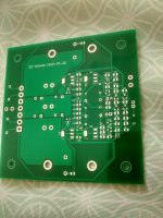
After a lot of hassle with AllPCB, DHL express and the customs I finally received the PCBs. As a result AllPCB now is on my personal "ignore list".
Attachments

Last edited:
Hi Voltwide,
How is the quality of these PCBs? I've ordered many PCBs from Chinese but there is no anywhere i actually feel OK.
Regards,
Cuong Nguyen
How is the quality of these PCBs? I've ordered many PCBs from Chinese but there is no anywhere i actually feel OK.
Regards,
Cuong Nguyen
Hi Voltwide,
How is the quality of these PCBs? I've ordered many PCBs from Chinese but there is no anywhere i actually feel OK.
Regards,
Cuong Nguyen
I use JLCPCB mostly but have used PCBWAY.
The quality has been amazing even on fine scale SMD with very small via's.
I sometimes get JLCPCB rejecting my files for silly reasons.
I just resend the same files and next time someone different scans them and they go through.
nice project.
just curious to know if have you looked at the clipping behavior?
mlloyd1
Thank you. I did not check this seriously in simulation - waiting for real result to come. But there will be 2 clamp diodes providing unsaturated clipping in case the driver circuit will be fed by some bootstrapped supply (refer to aux supply).
Last edited:
I use JLCPCB mostly but have used PCBWAY.
The quality has been amazing even on fine scale SMD with very small via's.
I sometimes get JLCPCB rejecting my files for silly reasons.
I just resend the same files and next time someone different scans them and they go through.
The trouble with Allpcb was they offer "DHL" - but they send by DHL-express. Being asked they strictly deny DHL-express - although I have the 1.hand information from DHL-express that AllPCB is their customer. So, whom do you think I will believe?

- Home
- Amplifiers
- Solid State
- Just another lateral FET amp