By way of background, I've been intrigued by some of the very simple amplifier circuits presented here, and have wanted to explore quasi-complimentary designs for several months now.
Inspiration for this project has come from Gareth (TGM lineup), Hugh (AKSA-55) and Carlos (original DX amplifier). I had originally planned to assemble Quasi's Nmos200; however, difficulties procuring boards has left me with a bag of IRF840 MOSFETs and nowhere to turn!
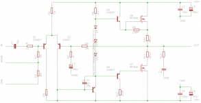
The schematic I present is as simple as I can possibly make it, without comprosing it to the point where it is just a giant oscillator. If you can think of any way to reduce the parts count further please let me know. Likewise, if I've omitted something essential for function or stability I'd like to know too.
I know there are 101 ways I can make this 'better': CCS on the LTP, degen resistors, bootstrap or CSS on the VAS, RC filters on the rails, etc. For this project I want to keep it as simple as possible and then my next project will be to embellish this circuit with some extra features.
Please let me know if there's anything I've missed (noting my Keep it Simple design ethos) and check my R values.
Next step will be to prepare a board layout and send the Gerber files to my board house.
Edited 30 September 2016:
Please refer to the post #1384http://www.diyaudio.com/forums/soli...mentary-mosfet-amplifier-139.html#post4844098 for the latest circuit:
http://www.diyaudio.com/forums/soli...mentary-mosfet-amplifier-139.html#post4844098
Inspiration for this project has come from Gareth (TGM lineup), Hugh (AKSA-55) and Carlos (original DX amplifier). I had originally planned to assemble Quasi's Nmos200; however, difficulties procuring boards has left me with a bag of IRF840 MOSFETs and nowhere to turn!
The schematic I present is as simple as I can possibly make it, without comprosing it to the point where it is just a giant oscillator. If you can think of any way to reduce the parts count further please let me know. Likewise, if I've omitted something essential for function or stability I'd like to know too.
I know there are 101 ways I can make this 'better': CCS on the LTP, degen resistors, bootstrap or CSS on the VAS, RC filters on the rails, etc. For this project I want to keep it as simple as possible and then my next project will be to embellish this circuit with some extra features.
Please let me know if there's anything I've missed (noting my Keep it Simple design ethos) and check my R values.
Next step will be to prepare a board layout and send the Gerber files to my board house.
Edited 30 September 2016:
Please refer to the post #1384http://www.diyaudio.com/forums/soli...mentary-mosfet-amplifier-139.html#post4844098 for the latest circuit:
http://www.diyaudio.com/forums/soli...mentary-mosfet-amplifier-139.html#post4844098
Attachments
Last edited:

two initial comments:
biasing for Q5 looks dodgy - missing a resistor i think.
Q3 needs to be fed from junction of Q1 and R5 - looks like a typo.
biasing for Q5 looks dodgy - missing a resistor i think.
Q3 needs to be fed from junction of Q1 and R5 - looks like a typo.
Last edited:
FET's are voltage driven rather than current drive which means you can not connect the gates as shown. Q5 is wrongly connected too. It should be from "gate to output", not gate to source. As it is now it can only pull the gate down, not turn it on. Also you need "gate stopper" resistors in series with the FET gates mounted as close to the FET's as possible.
Thanks kasey and mooly, I'll update the schematic shortly. Are gate stoppers strictly required or just recommended for stability?
Gate stoppers are essential, not an option. Use something like 270 or 330 ohm on a design like this.
Mooly, would you please explain the function of the gate stops and your reasoning for the large value? The stoppers on quasi's nmos design are only 27R. Thanks
Q5 emitter to OUT, collector to mosfet gate, R12 gate to source like R9.Q5 is wrongly connected too. It should be from "gate to output", not gate to source.
Also if you increase the value of R9 enough you might be able to eliminate Q4.
Also put R11 in Q7 source lead, not drain.
Bone - thanks for the reference to Nelson Pass' project. Reading this article and studying several other schematics from this vintage, I believe the performance will be inadequate without a bootstrap on the VAS.
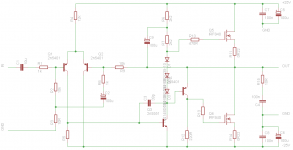
All - updated schematic attached. Is this workable? How to I go about optimizing the values of R10, R12 and R13?
Any thoughts on how best do I determine the required bias voltage?
thanks
All - updated schematic attached. Is this workable? How to I go about optimizing the values of R10, R12 and R13?
Any thoughts on how best do I determine the required bias voltage?
thanks
Attachments
Mooly, would you please explain the function of the gate stops and your reasoning for the large value? The stoppers on quasi's nmos design are only 27R. Thanks
Higher values will "play safe" and make the design more tolerant of any compromised layout and so on. That was my reasonlng. It removes a potential source of trouble for you.
Bone - thanks for the reference to Nelson Pass' project. Reading this article and studying several other schematics from this vintage, I believe the performance will be inadequate without a bootstrap on the VAS.
All - updated schematic attached. Is this workable? How to I go about optimizing the values of R10, R12 and R13?
Any thoughts on how best do I determine the required bias voltage?
thanks
Yes, its workable although it may need need more refinement to get the very best from it.
Oh yes, nearly forgot 😀
Bias. it would be much better (more thermally stable) with a proper vgs multiplier in place of the diodes. You could just copy a normal bjt transistor one (one NPN transistor, one resistor and one preset) and use that. The transistor must be in thermal contact with the heatsink.
Bias. it would be much better (more thermally stable) with a proper vgs multiplier in place of the diodes. You could just copy a normal bjt transistor one (one NPN transistor, one resistor and one preset) and use that. The transistor must be in thermal contact with the heatsink.
R14 is wrong, it should be between the output node and emitter/drain node.
R10 and 13 should be the same value. 470 as you have is a good starting point. 220 is also a good starting point for R10.
You will need an oscilloscope or simulator to optimise the values.
R10 and 13 should be the same value. 470 as you have is a good starting point. 220 is also a good starting point for R10.
You will need an oscilloscope or simulator to optimise the values.
With these, always a good idea to look at what the circuit is doing open loop as well. Just so you know what goes into the sausage 😉
Member
Joined 2009
Paid Member
MOSFETs are finicky things, they will oscillate just if you look at them funny... in addition to gate stoppers I have included additional footprints on all my latest pcb's that use MOSFETs at the output to include an SMT zobel network between gate and drain. A series R and C. You don't have to populate the pads, but they are there if needed or if you end up trying a particular MOSFET that's more finicky than the others. Put some nice rail caps close to the FETs on the pcb too.
Depending on which MOSFET you want to add gate protection zener diodes - most MOSFETs need them.
I would also allow space for lead compensation, a small cap from VAS collector to the feedback node.
I'd add a resistor (e.g. 82R) in the power rails with cap to ground, to isolate the front end from the power output stage. This is fairly common, to avoid unintentional feedback via the power rails.
Sorry - I added so many parts !!!!
Last edited:
Although not a quasi, if you look up International Rectifier Application Note AN-948 you will find a nice and simple worked example of a HEXFET amp together with a simple board layout.
Member
Joined 2009
Paid Member
I agree with Mooly's suggestion for the LTP tail resistor (your R4, his R2) which shoudl be 22K not 12K. This does cut the current through each transistor in half but it allows the collector load resistor to be twice as large in value which helps push up the open loop gain. Although less current means less slew rate, you can ameliorate somewhat this issue if you keep Cdom small by adding the lead compensation cap I mentioned already.
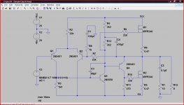
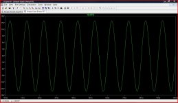
This works at a basic level. It needs the bias network adding 🙂
Very generous of you to take the time to simulate this. Any chance you would send me the files to play with?
MOSFETs are finicky things, they will oscillate just if you look at them funny... in addition to gate stoppers I have included additional footprints on all my latest pcb's that use MOSFETs at the output to include an SMT zobel network between gate and drain. A series R and C. You don't have to populate the pads, but they are there if needed or if you end up trying a particular MOSFET that's more finicky than the others. Put some nice rail caps close to the FETs on the pcb too.
Depending on which MOSFET you want to add gate protection zener diodes - most MOSFETs need them.
I would also allow space for lead compensation, a small cap from VAS collector to the feedback node.
I'd add a resistor (e.g. 82R) in the power rails with cap to ground, to isolate the front end from the power output stage. This is fairly common, to avoid unintentional feedback via the power rails.
Sorry - I added so many parts !!!!
I can see you are conspiring to turn my simple amplifier into a complicated beast 😀
The prospect of adding the 4 passive devices (even pads) for the zobel networks makes me very unhappy indeed 🙁 I need to read more about about the causes and remedies for parasitic oscillation in MOSFETs.
Bob Cordell published a paper discussing the issue on his website here: CordellAudio.com - A MOSFET Power Amplifier with Error Correction I'm hopeful that with only a single pair of outputs, the relatively high gate stopper resistances in this design, close decoupling around the source/drain and careful PCB layout will save the day. But I will take your suggestion under advisement and may incorporate it in the PCB layout after further research.
I plan to put place rail decoupling caps as close to the MOSFETs - as large and as close as practical. My aim is to lay out a 2ch amplifier on a single 10x10cm board. Ideally I'd like the bulk filter caps onboard (say a 4,700uF cap per rail per channel) but if space constraints dictate otherwise, I'll move the bulk caps offboard and put some 100-220uF decoupling caps there instead.
I'll give serious consideration to the gate-source protection diodes, thanks for the suggestion. I'm a little perplexed that the large majority of MOSFET designs here (including Quasi's popular Nmos project) omit this protection.
On a different note, you might be pleased to know I've decided to give the LTP a fighting chance by adding a modest RC filter to the +ve rail between the VAS and the tail resistor.
Although not a quasi, if you look up International Rectifier Application Note AN-948 you will find a nice and simple worked example of a HEXFET amp together with a simple board layout.
Thanks again Mooly. This is almost exactly what I want to build (substituting a quasi output stage for the complimentary pairs).
I agree with Mooly's suggestion for the LTP tail resistor (your R4, his R2) which shoudl be 22K not 12K. This does cut the current through each transistor in half but it allows the collector load resistor to be twice as large in value which helps push up the open loop gain. Although less current means less slew rate, you can ameliorate somewhat this issue if you keep Cdom small by adding the lead compensation cap I mentioned already.
Sounds like good advice to me and I'll adopt the 22k for the tail resistor. Mooly has also increased the feedback network attenuation in his Spice model to give a more reasonable closed-loop gain - something that was on my "to do" list - noted and adopted.
I'm interested in playing with the Cdom value and experimenting with lead comp once I can get this thing into Spice.
DMMT5401
I will likely follow in Gareth's footsteps and lay this out using a combination of SMT and TH devices.
I stumbled across this part in a SOT-32-6 outline and thought it would be ideal for the LTP since it comprises two "super matched" 5401 NPN transistors in a single package. A quick search here revealed that AKSA have used this in some of their designs.
http://www.diodes.com/datasheets/ds30437.pdf
Are there any downsides apart from the reduced Pd, which won't be an issue for me in this application. Frankly I'm surprised this device isn't more widely used considering how important a close match is for the diff amp transistors.
- Home
- Amplifiers
- Solid State
- Very simple quasi complimentary MOSFET amplifier