Hi everyone,
I'd like to share my latest project — a fully custom digital audio processing platform built around an FPGA. The system accepts multiple digital audio inputs (I2S/SPDIF), applies jitter reduction and fixed-point filtering, and outputs a balanced signal through a discrete R-2R DAC.
The goal was to achieve low-jitter, low-distortion output using hardware-domain techniques, while maintaining maximum flexibility in digital audio processing.


🎶 Subjectively, the system sounds clean, fast, and airy — with a notably improved low-end and clarity after FIR+ASRC stages. THD harmonics are drastically reduced when reclocking and passive output filters are tuned properly.
📎 I'm later to share code, VHDL modules, schematics, and REW test plots if anyone’s interested. Feedback, suggestions, and collaboration are very welcome!
Best regards,
Erdal
I'd like to share my latest project — a fully custom digital audio processing platform built around an FPGA. The system accepts multiple digital audio inputs (I2S/SPDIF), applies jitter reduction and fixed-point filtering, and outputs a balanced signal through a discrete R-2R DAC.
The goal was to achieve low-jitter, low-distortion output using hardware-domain techniques, while maintaining maximum flexibility in digital audio processing.
🔧 Hardware Specs:
- FPGA: Altera Cyclone IV EP4CE115
- Inputs: I2S (from XMOS, HDMI, STM32), SPDIF (optical & coax)
- Output: Balanced R-2R DAC (via 74LVC595 shift registers, isolated with SI8660)
- Clocks: External 22.5792 MHz & 24.576 MHz oscillators, dual PLLs with dynamic reconfiguration
🧠 Signal Processing Chain:
- ✅ Sample rate detection: 44.1 kHz to 384 kHz (auto-detect)
- ✅ Bit depth detection: 16-bit / 24-bit
- ✅ I2S Reclocking: FIFO-based low-jitter BCLK generation
- ✅ Fixed-point FIR Filter: Linear phase, group-delay-aware, designed for steep roll-off and minimal ripple
- ✅ ASRC (Asynchronous Sample Rate Converter): Linear interpolation based, upsampling to fixed 192 kHz / 24-bit output
🔊 Analog Output Path:
- DAC type: Discrete R-2R, balanced
- Output filter: Passive RC (887 Ω + 3.3 nF → fc ≈ 54 kHz), optimized via REW tests
- Preamp: OPA627, gain x2, input RC filter (1k + 470 pF)
🧪 Measurement Results (REW):
- SNR: 81 dB
- ENOB: 12.6–12.8 bits
- THD+N: ~0.018% @ 1 kHz, -1 dBFS
- Tested Scenarios:
- FIR only
- Reclock only
- FIR + Reclock
- Raw (flat path)
- Interesting Findings:
- THD increases at 44.1 kHz compared to 192 kHz due to increased jitter sensitivity
- RCA measurements underreport performance due to lack of CMRR; balanced output performs better
🚧 Current & Future Work:
- ASRC output working on (fixed 192 kHz)
- Next step: porting design to Xilinx Artix-7 (100T)
- Native DSD passthrough & PCM-to-DSD conversion under development
- DSD dac by upper PCB
🎶 Subjectively, the system sounds clean, fast, and airy — with a notably improved low-end and clarity after FIR+ASRC stages. THD harmonics are drastically reduced when reclocking and passive output filters are tuned properly.
📎 I'm later to share code, VHDL modules, schematics, and REW test plots if anyone’s interested. Feedback, suggestions, and collaboration are very welcome!
Best regards,
Erdal
Attachments


Hi Erdal,
May I ask for more clarification on what your overall goal for this project is?
You did say low jitter, but I don't see clear evidence of very-low jitter circuitry in the pics you have shared? I mean, it looks like you could do a lot more optimization to reduce jitter. And if jitter is semi-low then Vref is the other critical reference signal, so what about that? Getting those two things to a better state, then better isolation of the dac section from the DSP section could probably help a lot with achieving lower distortion and noise.
Of course, the DSP will probably have to get better too. If you might be interested, there is an interesting article in the forum about ASRC design with poly-phase filters by forum member Werewolf. Moreover, some ASRC designs have gone so far as to provide adaptive length FIFO buffering before the ASRC to allow a lower corner frequency for the PPLL (Polyphase PLL).
The other impression is that this is maybe more about just having fun designing something.
Best,
Mark
Last edited:
Always nice seeing new projects 🙂
My question is about fpga, why use such an expensive one? What are the benefits versus much less priced ones?
My question is about fpga, why use such an expensive one? What are the benefits versus much less priced ones?
Hi Mark,
Thank you for your thoughtful response — I really appreciate your observations.
You're right to note that the current photos and measurement results may not fully represent an ultra-low jitter implementation. The core intention behind this project is a mix of two goals:
To explore and develop a full digital audio pipeline in FPGA from the ground up, including:
Sample rate and bit depth detection
FIFO-based reclocking
Fixed-point FIR filtering
Linear interpolation ASRC (development process)
And a discrete, balanced R-2R DAC output stage
To maintain a practical, DIY-friendly approach using widely available parts, while still achieving respectable performance (SNR >80 dB, ENOB >12.5 bits, THD+N ~0.018%).
That said, you're absolutely correct — there's a lot of room for improvement in the analog layout, clocking architecture, and DAC isolation. This is something I'm actively iterating on. For example:
I’ve just received 1 ppm TCXOs (24.576 MHz) to replace the current clock sources and reduce overall PLL phase noise. And I am planning to develop si5340 or crystec femto clock
I'm planning to shift the design to an Artix-7 FPGA, which will allow tighter control of internal clock routing and potentially reduce jitter at the I2S generation stage.
Analog and digital power domains will be separated more rigorously in the next revision (with improved grounding and isolated power for the DAC).
The output stage will eventually include an op-amp buffer with properly designed analog filtering, something currently missing in my discrete R-2R DAC implementation.
For now, the goal is to establish a reliable baseline that can be measured, iterated upon, and eventually enhanced.
And yes — you’re absolutely right again: a big part of this project is just the joy of building, testing, and learning by doing. Having fun with audio DSP on real hardware is half the motivation
Thanks again for the insights, and I’m always open to suggestions if you see areas that can be tuned further!
Best regards,
Erdal
short answer, to be able to add more features. FIR Filter consumes too much resources (40-50k LE)Always nice seeing new projects 🙂
My question is about fpga, why use such an expensive one? What are the benefits versus much less priced ones?
Hi Erdol,
Basically, TCXO is not the most correct clock type for audio. Temperature compensation is not really needed since long term frequency stability is not as important as low close-in phase noise. On that latter point, clocks specified for low jitter at 12kHz offset and above (offset from the "carrier" that is, in this case the carrier refers to the nominal clock frequency), are also not well specified for audio. The lowest cost audio grade clocks are probably the NDK SDA series, although they may be sensitive to air current temperature stability issues. Maybe a little better is Crystek 957 (although they have been found sensitive to bypass capacitor type). Also, IMHO Si clocks are not that ideal for audio. They used to include phase noise plots in the datasheets, but may have found it found it better for sales to hide that information in a hard to find application note document.
Regarding the overall subject of clocking, external clocks, reclocking, squaring of sine wave oscillators, use of ferrite bead power filtering, etc., you might find my clock board thread of some interest: https://www.diyaudio.com/community/threads/general-purpose-dac-clock-board.413001/
Also, there is a simplified and more compact design example at: https://www.diyaudio.com/community/...2soverusb-pcm2dsd-rtz-dac.423401/post-7917601
On the subject of linear interpolation ASRC, it may be necessary to upsample quite a bit before interpolating if distortion is to be kept low. However, that then creates another set of problems to be solved. The article by Werewolf explains quite well: https://www.diyaudio.com/community/threads/asynchronous-sample-rate-conversion.28814/ The author's credentials are available: https://www.diyaudio.com/community/threads/asynchronous-sample-rate-conversion.28814/post-333645
Best Regards,
Mark
Last edited:
First of all congratulations on making a complex project like this work at all! It is no small feat! Now you have a great platform for further experimentation and learning. Looking forward to seeing more of the design.
Br
OJG
Br
OJG
Thank you OJG. It is a project that is open to development. FPGA provides flexibility. I also designed the FPGA board as a module. And I also have an artix7 pcb that I haven't soldered up yet.
The hardware and output design on it is more advanced than commercially produced r2r dacs. I used lt3042's in analog supply. I used lvc245 between lvc595's and resistor network and paralleled their outputs. (to reduce the internal resistances of the sink and source)
The analog supply (lvc) is bipolar +- 2.25 volt, so no ofset on output.
As I said above, there are si8660's between the digital (FPGA) and analog sides.
Not uncommon. However, makes me wonder if you listen to the sound of that compared to other low-ish noise regulators? Some people feel that the noise spec of a regulator is not the only thing that matters. OTOH, @MarcelvdG designed a fine sounding low noise regulator based on bandgap design followed by a low noise opamp and discrete output stage for his RTZ dac.I used lt3042's in analog supply.
IMHO, the problem with some of this stuff, and that includes Si clocks, is that people believe the sales pitch that is designed into datasheets by the IC manufacturer's marketing department. As always, its up to the buyer to beware and make sure the product is really the best fit for a given project. Sometimes only in-circuit evaluation can provide that information. Also, for audio use where the aim to to please human listeners, listening tests may be appropriate, but its a whole 'nother subject that's too complex to describe in one post.
hi again,
I reduced snr and thd a bit more by optimizing vhdl a little bit.

I also made it possible to play DSD directly by adding the DSD upper pcb.

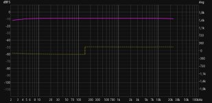
My test with FIR filter and no FIR filter. At 20,000 Hz cut-off frequency


I am currently working on ep4ce115 as FPGA. I hope to get better results with Artix7-100t.

The reclok module works but since it is not a quality osc there is no significant change. I plan to try it with the crystek (or si5xxx) modification in the future.
I am currently working on ASRC. There have been some revisions on the PCB. I plan to share the codes and schematics with the revisions in the future.


Best regards,
ERDAL
I reduced snr and thd a bit more by optimizing vhdl a little bit.
I also made it possible to play DSD directly by adding the DSD upper pcb.
My test with FIR filter and no FIR filter. At 20,000 Hz cut-off frequency
I am currently working on ep4ce115 as FPGA. I hope to get better results with Artix7-100t.
The reclok module works but since it is not a quality osc there is no significant change. I plan to try it with the crystek (or si5xxx) modification in the future.
I am currently working on ASRC. There have been some revisions on the PCB. I plan to share the codes and schematics with the revisions in the future.
Best regards,
ERDAL
OTOH, @MarcelvdG designed a fine sounding low noise regulator based on bandgap design followed by a low noise opamp and discrete output stage for his RTZ dac.
Do you have a link or schematic?
Here you are building both of the discrete DAC projects I've been wanting to do, and you are putting both in the same project!
A few questions I have:
Do you have THD measurements of DSD DAC? If you don't know already, you can use foobar2000 and it's dsd plugins to generate dsd test signals.
Do you use sign-magnitude for the R2R DAC? How do you minimize glitches?
Why will the Artix7 be better than the EP4?
A few questions I have:
Do you have THD measurements of DSD DAC? If you don't know already, you can use foobar2000 and it's dsd plugins to generate dsd test signals.
Do you use sign-magnitude for the R2R DAC? How do you minimize glitches?
Why will the Artix7 be better than the EP4?
Its in the schematics for his RTZ dac. You know the thread. First post has links to the schematic.Do you have a link or schematic?
I did a DSD listening test with foobar2000 but I haven't measured it with REW yet. No any audible glitches or noiseDo you have THD measurements of DSD DAC? If you don't know already, you can use foobar2000 and it's dsd plugins to generate dsd test signals.
I have a VHDL module that converts two complement i2s data to sign-magnitude. But I need to work on it. It is not exactly what I want. The measurement results are without this module.Do you use sign-magnitude for the R2R DAC? How do you minimize glitches?
I also put a 100uF + 100nf capacitor between each LVC vcc to gnd. And make a sensitive zero crossing adjustment with a trimpot in the part where the MSB bit is.
I did't use any DC blocking capacitors at the output. Because the LCV's use symmetrical supply and the common point GND.
EP4C is an old technology FPGA. Artix7 is better at timings. Especially the PLL part is much more advanced. It has low jitter.Why will the Artix7 be better than the EP4?
This will be very useful for me in the Reclock and ASRC part. Let me tell you about one difference. Since Artix7's PLL can do fractal multiplication and division, it can produce all sample rates with a single 24.5760000 mhz osc.
Maybe fine for anything except radar and audio. Timing jitter is a real thing in dacs, just as Vref noise is a real thing. Both jitter and Vref noise are multiplicative, not additive, with the audio signal. Any noise or other errors in those two analog signals (clocks ARE analog signals, NOT digital), will produce noise sidebands (intermodulation products) as seen in noise skirts around the base of FFT spectral lines. You know about this stuff, right?....it can produce all sample rates with a single 24.5760000 mhz osc.
Of course I know this is not ideal. I gave this example to show that while it is impossible in EP4CE, it is "possible" in Artix7.You know about this stuff, right?
As jitter increases exponentially, why not use a FPGA with lower jitter and traces?
Makes sense, at least to some extent. However, IME at least, for best results an FPGA will never be low jitter enough without some synchronous reclocking after the FPGA and before the dac.
I forgot to mention something. I am doing MSB bit inversion using LVC1g04Do you use sign-magnitude for the R2R DAC? How do you minimize glitches?
I made a mistake 🙁Do you have THD measurements of DSD DAC?
When R2R DAC is working (PCM), I separate DSD pcb from output with relays. There is no problem in this section. However, in the opposite case, that is, when DSD dac is active, R2R line is not separated. For this reason, 2 problems occurred;
1- If I make the outputs with LVCs /OE pins on r2r side HiZ, 1/2 vcc is on analog output.
2- If I do not do this, output offset does not occur, but the resistance line works as a 2.49 k resistor divider on output.
It works, but with some sacrifice of output amplitude
In such a complex project, mistakes are inevitable.
Best Regards,
ERDAL
- Home
- Source & Line
- Digital Line Level
- My FPGA based discrete R2R DAC Project