The OPA861 requires considerable care in the layout otherwise instabilities result. I gave up on it for now using an AD844 instead, though I suspect it could work very well.

I bought 6 of these off Aliexpress, since my AD844's were genuine thought what the hell lets roll the dice again.
From 3 different sellers, 2 each (to sample the market).
All 6 measure like this. Interesting almost pure 2nd harmonic.
+-10V rails - 0.7Vrms
Feedback resistor decreased from 1.5k to 1k, since 8mA DAC. However im not sure if its still too much current for AD811.

Anyone have any measurements using the schematic from post 1?
(Apologies if it was posted before, searching this thread for keyword "measurement" - 0 results containing image)
LCSC just got 50 in stock 2 weeks ago, for 12$ each. Might get some on next order just to make sure
From 3 different sellers, 2 each (to sample the market).
All 6 measure like this. Interesting almost pure 2nd harmonic.
+-10V rails - 0.7Vrms
Feedback resistor decreased from 1.5k to 1k, since 8mA DAC. However im not sure if its still too much current for AD811.
Anyone have any measurements using the schematic from post 1?
(Apologies if it was posted before, searching this thread for keyword "measurement" - 0 results containing image)
LCSC just got 50 in stock 2 weeks ago, for 12$ each. Might get some on next order just to make sure
Last edited:
The output current of the OP in I/V does not depend on the feedback resistor (at least at high load resistance), but only its output voltage.Feedback resistor decreased from 1.5k to 1k, since 8mA DAC. However im not sure if its still too much current for AD811.
Alex.
@Dendrobium , do you talk about the AD811 or AD844 ?
If AD811, 8 mA input, you could certainly reduce the feedback R at half of 1k5. So around 750R 🙂 Look at the datasheet, near ideal number for THD and stability !
The serie compensation cap could certainly reduced to 700 hz. maybe interresting to measure 1 K hz then 700 Hz for this serie input of the AD811.. Output serie resistor something from 10R to 20R ?
AD844, I have no idea, but the specs of the 861 that has near tipology are better everywhere (and marry well with signature like TDA1541A or AD1865)
What did you do in your layout, please ? Pedja Rogic chose simple ttaces near the signals' one as return path towards farer local star grounding ref plane.
If AD811, 8 mA input, you could certainly reduce the feedback R at half of 1k5. So around 750R 🙂 Look at the datasheet, near ideal number for THD and stability !
The serie compensation cap could certainly reduced to 700 hz. maybe interresting to measure 1 K hz then 700 Hz for this serie input of the AD811.. Output serie resistor something from 10R to 20R ?
AD844, I have no idea, but the specs of the 861 that has near tipology are better everywhere (and marry well with signature like TDA1541A or AD1865)
The OPA861 requires considerable care in the layout otherwise instabilities result. I gave up on it for now using an AD844 instead, though I suspect it could work very well.
What did you do in your layout, please ? Pedja Rogic chose simple ttaces near the signals' one as return path towards farer local star grounding ref plane.
Last edited:
Hi I have real ones if you want them. AD844 that is.
About AD811. I only mentioned the AD844 to say i also rolled the dice on Aliexpress, and (pretty sure) got real ones, so rolling dice on AD811 now and seeing if i got lucky again. Sorry for any confusion.@Dendrobium , do you talk about the AD811 or AD844 ?
And thank you Jean, you are kind 🙂 , but i think im covered on AD844 front.
If AD811, 8 mA input, you could certainly reduce the feedback R at half of 1k5. So around 750R 🙂 Look at the datasheet, near ideal number for THD and stability !
Interesting you say this, it seems true. I tried values from 470-1.5k, then adjusting input to match equivalent volume, and seems like there is really a noticable improvement in measuring, sweet spot around 820-1k value. I still have too much gain and i can hear a little noise on sensitive equipment, so i might drop little some more. I really dont listen loudly.
Yes, seems right, i have 10R now and no issues with stability. But might increase to 33R since im playing with AD8007 also, and it is far more difficult one to get a grip on. And i am basically doing worst case scenarios, driving 300pf cable with 18R load directly (yes not many mW but still).Output serie resistor something from 10R to 20R ?
After finnicking long time with AD8007 (same schematic)
Nice performance for 2Vrms i think, for such a simple scheme too. Keep in mind my interface input distortion is also in there (motu M2)
Was pretty hard to get stable though, this thing just wants to oscillate all day but got it there in the end

Have to recalibrate scale though, i changed USB inputs and now REW shows 2Vrsm as only -63dB (and noise in -180db, i wish that were true..)

Made on AD's XFCB process and 811 is CB process, so i guess it could be considered its grandfather. It's a nice part, this vs AD811 probably just academic, and 811 is proven already but why not play with others too.
Nice performance for 2Vrms i think, for such a simple scheme too. Keep in mind my interface input distortion is also in there (motu M2)
Was pretty hard to get stable though, this thing just wants to oscillate all day but got it there in the end
Have to recalibrate scale though, i changed USB inputs and now REW shows 2Vrsm as only -63dB (and noise in -180db, i wish that were true..)
Made on AD's XFCB process and 811 is CB process, so i guess it could be considered its grandfather. It's a nice part, this vs AD811 probably just academic, and 811 is proven already but why not play with others too.
Finally what -3 dB cut off did you choose in the feedback loop ? Still oscillate if you cut off at 20 K hz or 44 K hz ? 6 dB slope there too weak ?
Finally what -3 dB cut off did you choose in the feedback loop ? Still oscillate if you cut off at 20 K hz or 44 K hz ? 6 dB slope there too weak ?
I tried lowering the cut off, and there is an improvement of stability but increase volume enough and it would go again, so it wasnt good enough of a strategy to solve it i think.
Increased snubber (output resistor) to 20ohm helped, but increase volume some more and still it would go.
What ended up working is arrived experimentally. Basically broken up 1.5k into two parts, so cap is in series with some resistance, values not optimised at all here.
In sim this actually ruins HF performance of the feedback cap, now there's a resistor in series obviously.
Maybe it damps it somehow, changes some Q factor or whatever, if anyone knows i'd like to know as well.
Came by this post accidentally, maybe an interesting post from the old guard.
Hi DIY Audio Group and Johnego,
I have been doing this "audio stuff" a very long time and worked closely with great analog circuit engineers like Bob Pease at National Semi. I will tell you the LME49713 is the best sounding opamp we ever created on the very special LME high voltage process that is gone now. We did extensive listening sessions comparing VFB and CFB opamps and for most applications we preferred the LME CFB's (LME49713HA) with the exception sometimes being for +/- DAC outputs where the identical +/- inputs on the VFB opamps present identical loads to the DAC's. The +/- inputs on a CFB opamp are different input circuits.
Anyway we designed the LME49713HA CFB opamps to exceed the AD811 specs and made some significant changes to optimize it for audio (rather than video) but the bandwidth is still very high (which is a good thing for a lot of reasons) and thus requires careful PC layout to prevent oscillations. The AD811 was based on the AD9610 metal can mil spec opamps and one of the best measuring and sounding opamps ever...also super expensive and impossible to find. I still have a few for personal projects.
We attempted to do our critical listening tests (after all the measurement tests) single and double blind but there is always room for error/disagreement in all listening results.
Just wanted everyone on this forum to think/try VFB and CFB (voltage feed back vs current feedback) opamps in their new designs. I mentioned the older AD811 ADI CFB parts because the last I heard the LME high voltage process was shut down by TI.
Best “Retired” Audio Regards Everyone,
audioman54
Hi DIY Audio Group and Johnego,
I have been doing this "audio stuff" a very long time and worked closely with great analog circuit engineers like Bob Pease at National Semi. I will tell you the LME49713 is the best sounding opamp we ever created on the very special LME high voltage process that is gone now. We did extensive listening sessions comparing VFB and CFB opamps and for most applications we preferred the LME CFB's (LME49713HA) with the exception sometimes being for +/- DAC outputs where the identical +/- inputs on the VFB opamps present identical loads to the DAC's. The +/-...
I have been doing this "audio stuff" a very long time and worked closely with great analog circuit engineers like Bob Pease at National Semi. I will tell you the LME49713 is the best sounding opamp we ever created on the very special LME high voltage process that is gone now. We did extensive listening sessions comparing VFB and CFB opamps and for most applications we preferred the LME CFB's (LME49713HA) with the exception sometimes being for +/- DAC outputs where the identical +/- inputs on the VFB opamps present identical loads to the DAC's. The +/-...
From LME49713 (CFA) datasheet
Could be that the series resistor swamps the dynamic impedance of the capacitor with a much larger value than its own, or something like that. But just having that cap uninstalled also doesnt do it any good either, so i dont know.
CAPACITIVE FEEDBACK
It is quite common to place a small lead-compensation capacitor in parallel with a voltage feedback amplifier’s
feedback resistance, Rf. This compensation reduces the amplifier’s peaking in the frequency domain and damps
the transient response. Whereas this yields the expected results when used with voltage feedback amplifiers, this
technique must not be used with current feedback amplifiers. The dynamic impedance of capacitors in the
feedback loop reduces the amplifier’s stability. Instead, reduced peaking in the frequency response and
bandwidth limiting can be accomplished by adding an RC circuit to the amplifier’s input.
Could be that the series resistor swamps the dynamic impedance of the capacitor with a much larger value than its own, or something like that. But just having that cap uninstalled also doesnt do it any good either, so i dont know.
Thanks. That's interresting. Tested the ad811 in miro1360's thread but I am just at the beginning. Planned a benchmark of some OP amps at iso pcb layout and parts.
For voltage gain perhaps but does it apply to the transimpedance technic we are using where Cf is to limit the bandwith to compensate for the flatest response so transcient ? I see Cf here more like the needed evil as well as to have a flat impedance, so bigger value better, means low corner frequency but as I use NOS, - 6dB is anyway never really enough. In some VfB though a very low Cf and wide bandwith sounded better despite being fast op amp (AD9631)
But it is easy to test your theory by using a RC to ground before the input 1K R ?
I could test it with the AD811 on my last pcb, but Grunf tests seems to be okay with 1k5 and Cf.
Are you using smd parts and layout ?
Now there is maybe another way to see it : use small gain where the CFA is the more stable and use a second op amp to add voltage gain ? Preamp will do the rest. Is a too much I/V low gain a problem for micro/macro dynamic, errors or conversion ? We first need a low output flat impedance mostly...
Attachments
Last edited:
Yes, i suppose it should work and yes Rf does have a practical lower limit in CFB, unlike VFB where you can run unity gain without any resistor and be stable, in most CFB datasheets you will find 200-300ohm is needed at least, and also this is a useful document https://www.ti.com/lit/an/sboa095/sboa095.pdfNow there is maybe another way to see it : use small gain where the CFA is the more stable and use a second op amp to add voltage gain ? Preamp will do the rest. Is a too much I/V low gain a problem for micro/macro dynamic, errors or conversion ? We first need a low output flat impedance mostly...
No, and i have no good reason. SMD is better in basically every way and i have no problems soldering it. Just i guess i built up too much THT stuff and dont want to pull the trigger on transitioning.. and THT thin film resistors with 50ppm are kind of easily available today, but yes their parasitics are still worse. But i did use a kind of "RF-like" layout with 8 layers too making good use of all of them. But it is a trivial schematic so its not too difficult to do things by the book when there's almost no constraints bothering you.Are you using smd parts and layout ?
Yes for AD811 the shown values are fine, its a more stable, and slower and well behaved thingy. (assuming mine ad811 is even genuine, but i ordered 2 more this time from LCSC just to be sure, they seem to take it seriously at least never sold me anything fake thus far)I could test it with the AD811 on my last pcb, but Grunf tests seems to be okay with 1k5 and Cf.
I am worried with 47k load of Grunf and the 10R Rs for 100 pF shunt....
U have to try but perhaps a lower load from 1 to 10k R wouldbe better for Rs=30R witj 100pF shunt. But norhingimportant enough notto sleep withG shematic. A smd layout well made to figth stray capacitance and inductance matter more.
U have to try but perhaps a lower load from 1 to 10k R wouldbe better for Rs=30R witj 100pF shunt. But norhingimportant enough notto sleep withG shematic. A smd layout well made to figth stray capacitance and inductance matter more.
I assumed that 50k and 100p on page 1 schematic are just there as "R load" and "C load" for the sim, and not a part of the actual schematic.
10ohm is called an "isolation resistor" and isolates the opamp from the load. It is very common and you'll find it in any CFB datasheet. After it is just Rl and Cl which got baked into this schematic for some reason.
Its not meant as an RC with the 100p this much i know, its a 159 MHz (!) -3db (but, i dont know what your theory for it is).
Well the R load is fine to leave as it will not make a difference but just randomly driving a random 100p is not beneficial to any aspect of operation (though not terribly so, but it just adds in parallel to whatever cable you'll be driving).
But if it is part of the scheme after all, please explain its meaning.
Even if you want to include the R load, it will usually be on the input side of following device (preamp or amp or whatever), no need to add another one that will go in parallel with it.
Also making a design with small current return loops, stray capacitances and other is just good layout practice, nothing to do with SMD inherently, it was done for decades already before smd was around. It's just easier and better to do with SMD, on top of smd also having lower inherent parasitics. But a good layout is much more important than whether you choose to SMD or not.
Also i am already driving down to 15R (planar headphones) with it, with a 300pf cable, which is a crazy bad test load for it. Well for some it would be a 400pf cable, if they actually included a 100p cap in the schematic haha.
That's what I wrote here and believed it was the capacitance of the line plus the next stage load in the sim and asked, but see them later on the pcbs made... in the ad1862 thread. And G answerered it was for stability in a post above. Which can be I assume for higher capacitive load and due to the high slew rate speed of the AD811.... Datasheet says also transmission line should be 75 ohms terminated, so I assume 50 ohms for RCA cables. But voilà : my pre has a 220R in serie with input (and 47K shunt as a load ?!)
Yes Rs (10 ohms) is both an isolator for the load to prevent from too much capacitive and help also as compensation with Rfb (oscillation). Anyway it works fine w/o the 100p, but it should work better with 30R for Rs (look at fig 38 an AD811 datasheet)
Could be 47K loaded though for max power curent adaptation with a pre or amp with 47 k input ? But in case of modulated voltage signal across a transmission line, is 1/10 ratio not better, so more something like 4k7 at the DAC side. I always seen high impedance load on cd players but always after a DC isolation capacitor...
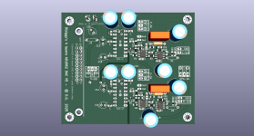
@Vunce, may you enligth us please. What did you do on your AD811 PCBs at the output ?
Yes Rs (10 ohms) is both an isolator for the load to prevent from too much capacitive and help also as compensation with Rfb (oscillation). Anyway it works fine w/o the 100p, but it should work better with 30R for Rs (look at fig 38 an AD811 datasheet)
Could be 47K loaded though for max power curent adaptation with a pre or amp with 47 k input ? But in case of modulated voltage signal across a transmission line, is 1/10 ratio not better, so more something like 4k7 at the DAC side. I always seen high impedance load on cd players but always after a DC isolation capacitor...
@Vunce, may you enligth us please. What did you do on your AD811 PCBs at the output ?
Hmm yes, i also saw on the PCB's made, i forgot who's but i guess it was Vunce. I wanted to ask but forgot so this is a good time then.
Well i think Vunce just copy pasted from schematic in post #1 (apologies Vunce if not true) so i am more interested why @grunf added it. He is making nice progress in Hiraga thread but now we're distracting him (well I am, haha), sorry grunf.
Any case someone copied the load from the datasheet into an actual scheme. Ok, maybe mistake, but lets clear it up now if it is.

But that's just to demonstrate how it does driving that load, not that you should put that load into the schematic
And , almost every other datasheet has a section about driving capacitive loads and what to do about it, and application notes written about it. https://www.ti.com/document-viewer/lit/html/SSZT999
But grunf knows a lot so i am also ready to potentially be enlightened 🙂
Well i think Vunce just copy pasted from schematic in post #1 (apologies Vunce if not true) so i am more interested why @grunf added it. He is making nice progress in Hiraga thread but now we're distracting him (well I am, haha), sorry grunf.
Any case someone copied the load from the datasheet into an actual scheme. Ok, maybe mistake, but lets clear it up now if it is.
Actually that's maybe how it happened...on fig 38 it has the same 100p value so maybe that's where the value chosen comes from.(look at fig 38 an AD811 datasheet)
But that's just to demonstrate how it does driving that load, not that you should put that load into the schematic
And , almost every other datasheet has a section about driving capacitive loads and what to do about it, and application notes written about it. https://www.ti.com/document-viewer/lit/html/SSZT999
But grunf knows a lot so i am also ready to potentially be enlightened 🙂
Last edited:
- Home
- Source & Line
- Digital Line Level
- AD811 as I/V stage for current DACs (and test some other opamps including Burson Audio opamps as I/V)