Hi All. I have the V4.2 boards and noticed the "surface mount" type solder points and a through hole. The legend says " ADJ33-100K". I 'm not sure really what is meant by them on this version board. Is this the position to replace the fixed resistor with a Trim-Pot please?


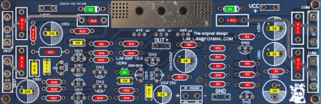
Looking at the board and schematic, it shows this is the position of R10 on the older boards. However, there is not any resistor in place at all on my V4.2 board, apart from the SM tabs as shown above... It seems odd there is no R10 on the board..... Perhaps LJM himself could explain, why this is so Please?


Ahhhh, I think it is starting to make sense. There is a new board position for R10 It is shown below. These SM tabs are there to make adding a trimmer pot easier if required. No need to remove and replace R19 now....just add the trimmer to the surface mount tabs!

I would greatly appreciate if anyone could confirm what I am suggesting. I just can't trace the printed circuit board. Also, could someone be so kind as show this mod as a new entry showing where and how to fit the trimmer and the value of it, please? Very much obliged. As suggested, I think this supercedes the earlier mod for the older boards.... Maybe something could be learned from the next version of the board, which is the VER 5, as this includes a trim-pot for bias adjustment as standard.
I'm a complete noob at this but I'm very interested in this amplifier. I have bought two pairs. One set is complete and the other is an unassembled kit. I will attach a photo of the bare PCB Version 4.2. Your schematic shows R10 as a 1k resistor but in the position on the PCB you have indicated as R10 it is a 10k resistor. I've also attached a photo I found online showing schematic positions on the PCB for version 4.
Attachments

I found this post on another thread which suggests the resistor you are indicating as R10 is actually R15.
https://www.diyaudio.com/community/threads/l12-2-cfp-output-amp-120w-2-8r.196089/post-7905192
Curious about the solder pads as the schematic for Version 4 shows the trimmer mod be placed in parallel with resister R19.
https://www.diyaudio.com/community/threads/l12-2-cfp-output-amp-120w-2-8r.196089/post-7905192
Curious about the solder pads as the schematic for Version 4 shows the trimmer mod be placed in parallel with resister R19.
Thank you very much SJKE. The bare PCB of V4.2 is very useful. As you can see the SM solder tabs correspond with R10. It will mean you can leave R10 (1K) in place and simply add a surface mount trimmer to the tabs to vary and adjust the bias current. I did message LJM for clarification but no reply as yet. It seems strange that LJM creates these newer versions but does let anyone know what to do with them. It would only require very little trouble to do so I think. By the way, I found the amplifier extremely detailed but too "bright" in my system. At the moment I prefer the L20 V 9.2. Thanks, please keep me updated on what you decide to do as regards the bias mods. Best regards.
Thanks for the reply sonicles. Prior to seeing your post, I assumed I would be removing R19 and applying the trimmer modification in it's place. However, what you propose seems like a much easier solution. On my examples the thru hole next to the solder pads is not open and I am not clear as to its function. I'll be happy to let you know what I come across. It's a slow process for me as I am starting this hobby from scratch. Not much in the way of supplies or components is readily available where I live. Aliexpress is unfortunately my easiest option. Thanks again.
I'm not brilliant with how the base voltage on the bias control transistors functions. It seems likely that if one adds a trimmer and leave the existing resistor (in parallel) it will "turn-on" the transistor a touch more as the base current is likely to increase. I wish someone could let me know for sure. I have also noticed the "through-hole" seems not to have any solder area either side of the board which seems a little odd. Maybe LJM might explain at some time .... fingers crossed. PS: Note there seems not to be any DC blocking capacitor on the input so you must check if your pre-amp has any DC component... even if it doesn't, I think a resistor of around 100K should be across the input as it is not on the board.On my examples the thru hole next to the solder pads is not open and I am not clear as to its function.
Attachments
I Have assembled the Accuphase C3850 clone and was planning on using it as my pre-amp. I measured the DC voltage at the output and both left and right channels measured -2mv. This was without a source signal supplied.Note there seems not to be any DC blocking capacitor on the input so you must check if your pre-amp has any DC component... even if it doesn't, I think a resistor of around 100K should be across the input as it is not on the board.
Surely those solder pads are there for a reason. Your assumption seems to be a logical one.As you can see the SM solder tabs correspond with R10. It will mean you can leave R10 (1K) in place and simply add a surface mount trimmer to the tabs to vary and adjust the bias current. I did message LJM for clarification but no reply as yet.
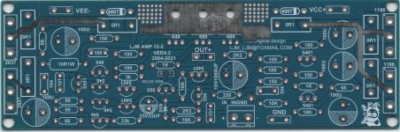
That pad with the hole next to the surface mount pad , 1st post second picture, could be a via to a trace on the other side of the board.
This is the other side of the board.That pad with the hole next to the surface mount pad , 1st post second picture, could be a via to a trace on the other side of the board.
Attachments

Looks like you will need a blocking cap at the input then. I think the easiest way is to have the capacitor (and resistor) at the RCA socket, then you can run the co-ax signal lead to the board as normal. I was going to use self-adhesive cable tie fixings to hold the large MKP type cap to the inside of the case. Not sure what value but used 10uF in my L20 amp. Obviously, it can go just at the input connector block on the board, but space could be very limited depending on your layout of the other components (PSU etc)I Have assembled the Accuphase C3850 clone and was planning on using it as my pre-amp. I measured the DC voltage at the output and both left and right channels measured -2mv. This was without a source signal supplied.
Yes .... also note the wording of: ADJ 33K to 100K .... seems a suggestion of the trimmer pot value?Surely those solder pads are there for a reason. Your assumption seems to be a logical one.
@sonicles
In my opinion your two recent threads, although not obviously, are closely related:
1. Harshness of sound is probably caused by crossover distortion
2. Bias adjustment can elliminate crossover distortion by adjusting a potentiometer parallel to R19
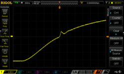
I have already verified that there is significant crossover distortion at default values. Please, observe a snapshot below. One can adjust biass current and consequently reduce the crossover distortion.
If you observe square wave response of L12-2 V4.2 and zoom in, you can observe a bulge right at the crossover point. It looks like a horn. By adjusting biass current one can practically zero crossover distortion. To do this you don't need to monitor THD values: just increase the biass current untill a bulge on square wave leading edge dissapears. This would eliminate harshnes of the sound.
In my opinion your two recent threads, although not obviously, are closely related:
1. Harshness of sound is probably caused by crossover distortion
2. Bias adjustment can elliminate crossover distortion by adjusting a potentiometer parallel to R19
I have already verified that there is significant crossover distortion at default values. Please, observe a snapshot below. One can adjust biass current and consequently reduce the crossover distortion.
If you observe square wave response of L12-2 V4.2 and zoom in, you can observe a bulge right at the crossover point. It looks like a horn. By adjusting biass current one can practically zero crossover distortion. To do this you don't need to monitor THD values: just increase the biass current untill a bulge on square wave leading edge dissapears. This would eliminate harshnes of the sound.
Attachments
Last edited:
Thanks very much Berlusconi. I have a pair of new boards and can do all the mods on that and compare. I do have a scope and sig gen with square wave o/p. I guess I'll do the "old" mod around R19 instead of wondering what the solder tabs are for in parallel to R10 then?

I'd be carefull here because just a slight error can cause extremely high current that might burn transistors. What is needed is: to replace R19 with a through-hole potentiometer adjusted to 1K initially. Then you can measure the desired resistor value and finally solder a fixed resistor in place of R19. Simple & safe.
Please observe the crossover distortion at the leading edge of the square wave response.

Please observe the crossover distortion at the leading edge of the square wave response.
I took another glance at the board just now. The values printed are ADJ33-100k. So is that 33R to 100,000R or 33,000R to 100,000R? I don't have any experience with these things. Is there a surface mount trimmer pot with that kind of range either way? As an experiment I just tested a trimmer pot I bought for the R19 modification. It has a range of 0-4.8K. No where near what would be needed. Or perhaps the trimmer pot is used to change the measured value from 33-100K at some other point on the board? Or could those pads just be a test point looking for a value between 33 and 100K. That doesn't seem likely though as some other component would need to be changed how many times to reach the desired effect? Too many questions.Yes .... also note the wording of: ADJ 33K to 100K .... seems a suggestion of the trimmer pot value?
I was thinking of using 2 conductor sheilded cable. Is coax, perhaps with a stranded core, a better option?then you can run the co-ax signal lead to the board as normal.
- Home
- Amplifiers
- Solid State
- L12-2 VER4.2 BIAS Control Pot position