As regards the unknown solder pads, I have now decided to ignore these and stick with the tried and tested original mod and replace R19 as per diagram above. I would suggest doing this to keep things simple. 2x conductor with shield is ok but using normal audio co-ax works well, plus you have a solid low resistance ground all the way from the preamp, right to the amp's input. Perhaps just stick with what you use for your pre-amp interconnect. With 2x toroidals, 2x PSUs and co-ax connections, I have ZERO hum and silent background.
Last edited:

Thanks for showing Berlusconi. I will be doing the mod very soon. Do you recall what bias you used to get the optimum low distortion and what output power was used, presumably in an 8- or 4-Ohm resistor load? Also, I have not added the output coil either, maybe that is not helping the bright sound? The amp currently runs very cooly.Please observe the crossover distortion at the leading edge of the square wave response
@sonicles
Thanks for sharing your thoughts, I do indeed appreciate that.
Now, I think I understand what 33-100K means: in other words it means that the additional SMD resistor should change resistance across R19 to be between 970R-1K (*). It should be understood that one should solder there a fixed value SMD resistor, not a potentiometer.
The reason for the necessity for meassurements is that there are variations in individual component values, hence different values are required for individual boards.
How to measure: just solder two isolated wires to the SMD pads and place a 100K potentiometer in series with 33K fixed resistor. The fixed value resistor is added to avoid accidental inrush of high current. Determine the optimal value by observing the leading edge of the square wave response.
Then simply de-solder these two wires along with resistors, meassure the resulting the overall resistance and replace that assembly with a SMD resistor of the closest value to the meassured. That's it.
(*) It is possible to calculate these values by applying simple Ohm laws.
Something similar I have published HERE
Last edited:
I think you have sold the mystery Berlusconi! Yes, by adding a resistor to the SMD pads with a range between 33K and 100K, you will change the value of R19 from between 970 - 990 Ohms. One could also solder a 100K Ohm trimmer to the same pads (with the wiper-leg across to one side leg). I went to the link you show above and realise I had missed all this detail. You show the optimum current to be around 22mA set by a 910 Ohm resistor. To get that lower figure we then need a TAB resistor of just 10K Ohm rather than only 33K Ohm, but then again 10K Ohm will be available if a 100K trimmer is used set to the high side initially for safety. Due to not wanting to continually remove the boards from the amplifier, I must make a choice of what way to physically do it, so I would prefer the trimmer soldered in option. Only thing I am not confident with is WHAT resistor on the 4.2 board is R19? please? It must be the one above and next to the 2x SMD tabs? PS: https://www.omnicalculator.com/physics/parallel-resistor PS: I must say just having a trimmer pot across the bias resistor is quite dangerous.... it really should have a series limiting resistor fitted as you describe above , as you could easily bypass the 1K Ohm resistor entirely if one adjusts the trimmer all the way to the wrong end.the additional SMD resistor should change resistance across R19 to be between 970R-1K
Last edited:
I found this in another post. It shows the location of R19. If you look at my bare board photo it shows this resistor to be a 1K resistor.Only thing I am not confident with is WHAT resistor on the 4.2 board is R19?
Attachments
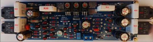
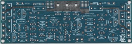
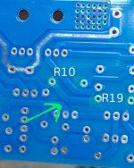
Excellent SJKE. Yes, the V4.2 layout shows that R19 has swapped position with R23 on the Ver 4.0 you show earlier. R19 and R10 measure 1K Ohm in the positions shown on V4.2. ... proving the latter one is correct ...(R23 is 100 Ohms) This is one reason I could not make sense of it. So, the tabs correspond to the R19 and thus make it easy to add a bias control resistor.... whether itI found this in another post. It shows the location of R19. If you look at my bare board photo it shows this resistor to be a 1K resistor.
be a trimmer or a fixed resistor... very well done and thanks 🙂
Last edited:
Hi SJKE...did some extra resistance checking and found that the SMD tabs MUST relate to the R10 resistor NOT R19!... It is easy to test. R19 gives me a reading of 999 Ohms but R10 AND the tabs give me an identical reading of 1003 Ohms making me pretty sure they are the very same. Try the test on yours. So, the design is to alter the resistance of R10 rather than R19, but I'm pretty sure either will have the same effect on varying the bias current.
Hey sonicles, I did some poking around with the continuity tester on my multimeter. I did rather jump around a bit but the points with the same color are connected. Maybe when I have some more time I'll try a more systematic method. R19 is connected to one pad and to R10. R10 is also connected to the other pad.
Attachments

R10 is connected to both pads, however, it is also connected to one pad in conjunction with R19.R10 AND the tabs give me an identical reading of 1003 Ohms making me pretty sure they are the very same.
Thank you very much "Sherlock". I have found that post too.I found this in another post.
I have found also a snapshot below in yet another post >HERE<.
Published by @dasoft
There is yet another very important post by @dasoft >HERE<
According to that post R19 should be 875 Ohms
It appears that I have re-discovered America. Good to know.
Also, I have been participant in that conversation but have forgotten everything - all gone with the wind.
Forgetfulness is Lords' Gift.
Last edited:
Excellent and thank you Berlusconi. I am now tempted to simply select an 875 Ohm (or the closest available combination) resistor rather than bother with the trimmer. PS: 510 + 360 (in series) = 870 Ohms.... tested selections will achieve desired 875 OhmsAccording to that post R19 should be 875 Ohm
Last edited:
Let me first quote myself :
I have re-evaluated my opinions today and can say that anything between 800 Ohm and 1K will be OK for L12-2.
LJM is indeed a good designer. We do not appreciate that enough. Even with the default values, i.e. without any changes, his board will be able to attain theoretically decent values of bias current. Read the quote below to see why. One can adjust the biass to even higher values if desired. Higher values will elliminate posiible cross-over artefacts. This has potential to make the board perform even better at the cost of even higher heat dissipation. Frankly, heat dissipation of this amplifier is modest taking into account the power it is capable attaining.
Here I will re-publish my previous post about L12-2:
Indeed, this is how we have capability to erase "facts" from our minds and addapt to the reality. Lord was indeed gracious. We can forget, let go, adapt and make room for new ideas.Forgetfulness is Lords' Gift.
I have re-evaluated my opinions today and can say that anything between 800 Ohm and 1K will be OK for L12-2.
LJM is indeed a good designer. We do not appreciate that enough. Even with the default values, i.e. without any changes, his board will be able to attain theoretically decent values of bias current. Read the quote below to see why. One can adjust the biass to even higher values if desired. Higher values will elliminate posiible cross-over artefacts. This has potential to make the board perform even better at the cost of even higher heat dissipation. Frankly, heat dissipation of this amplifier is modest taking into account the power it is capable attaining.
Here I will re-publish my previous post about L12-2:
Important Correction to this thread
Please, read carefully the following text because the entire thread reiterates wrong and confusing information about biassing of the output transistors.
First, to be precise, the L12-2 has CFP output pairs. The optimum quiescent current Iq across each emitter resistor in a CFP configuration is 10.3mA according to DF96 (a three-part article in Wireless World, in Sept, Oct and Nov 2000); Self found 11.5mA.
Also, the measurement procedure proposed here is wrong. Bias adjustments of PNP transistors should be based on voltage measurements between the Vcc and the emitters of Q2 or Q10. Similarly, bias adjustments of NPN transistors should be based on measurements between the Vee and the emitters of Q14 and Q18.
Today I have performed a series of THD measurements for different values of R19. It appears that there are no benefits whatsoever from increasing the quiescent current i.e., replacing the R1 with a potentiometer. The increase of the quiescent current just increases heat dissipation, nothing else, except, maybe, a pleasant effect of Placebo. Furthermore, the original value of the R19 is optimal hence there are no benefits from meddling with it.
LJM is a mature expert and he was constantly reiterating: this amplifier is good by design, there is no need to change anything – he knew better. Meanwhile he incrementally improved L12-2 by replacing C5 with the 33uF capacitor which has significantly reduced low frequency roll-off. Now, frequency response is flat like a pancake even over the boundaries of the audible region. Indeed, there is a slight high frequency boost, but insignificant an beyond the audible region.
Conclusions:
do not replace R19 .
do not replace C5 (except you have something very special)
this amplifier is good as-is by design
If you want to verify correctness of the bias do it with a multimeter with one probe on Vcc and another probe on the emitter lead of the PNP transistor. Similarly, you may verify the bias of the NPN transistors between the Vee and the emitter lead. Voltage loss across the emitter transistors would be 1.1-1.2 mV (11-12 mA across 0.1 Ohm resistor). Note also that, strictly speaking, measuring the quiescent current over R13 and R20 is wrong – it doesn’t account for Q5 and Q9 contribution to the overall Iq value.
I hope this helps
While I believe this to be the best way, I might resort to using a SMPS to get started. I'm starting from nothing and I want to power up and test the boards before I commit sourcing transformers. Shipping to Chile is expensive! But these questions are off topic and are best discussed in a different thread.With 2x toroidals, 2x PSUs and co-ax connections, I have ZERO hum and silent background.
Buongiorno, sono un nuovo iscritto, allego 2 foto, ho la versione 4 del l12-2 la resistenza del bias é da 1 kohm, é quella cerchiata in foto proprio supra la scritta ljm amp verso 4

Please post in English.
Translation:
Hello, I am a new member, I attach 2 photos, I have version 4 of the l12-2 the bias resistor is 1 kohm, it is the one circled in the photo right above the writing ljm amp towards 4
- Home
- Amplifiers
- Solid State
- L12-2 VER4.2 BIAS Control Pot position