This is Binjo's Experimental Amplifier (Non-Switching).
It's a concept based on a possibly original idea I had for driving MOSFETs, realised in the form of a non-switching amplifier.
As you can see, she's not like the other girls. She may not be Blameless, and possibly a naughty little minx, guilty on all charges.
I've been kinda working on this for a few years (on-and-off, mostly off) and now it's ready to share.
Output is 50W into 8 ohms. 100W into 4 ohms seems fine too.
Supply rails are +- 32V for the MOSFETS, +- 44V @ 100mA for the rest.
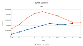
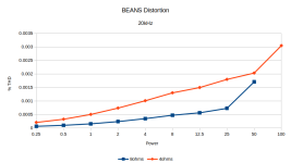
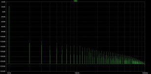
Distortion is:
0.000012% at rated power, 1kHz 50W into 8 ohms,
0.0017% at rated power 20kHz 50W into 8 ohms .
Slew rate 60V/uS
Frequency response -3dB @ 2.95 MHz
I've tried to get everything right, but for sure some things are amiss. If it were ever to be built, various things need adding: Protection, pre-amp stage, filtering, power supplies etc. I'm thinking of designing some of those bits next.
I'll add more info into this thread in due course.
It's a concept based on a possibly original idea I had for driving MOSFETs, realised in the form of a non-switching amplifier.
As you can see, she's not like the other girls. She may not be Blameless, and possibly a naughty little minx, guilty on all charges.
I've been kinda working on this for a few years (on-and-off, mostly off) and now it's ready to share.
Output is 50W into 8 ohms. 100W into 4 ohms seems fine too.
Supply rails are +- 32V for the MOSFETS, +- 44V @ 100mA for the rest.
Distortion is:
0.000012% at rated power, 1kHz 50W into 8 ohms,
0.0017% at rated power 20kHz 50W into 8 ohms .
Slew rate 60V/uS
Frequency response -3dB @ 2.95 MHz
I've tried to get everything right, but for sure some things are amiss. If it were ever to be built, various things need adding: Protection, pre-amp stage, filtering, power supplies etc. I'm thinking of designing some of those bits next.
I'll add more info into this thread in due course.
Attachments
Last edited:

I think you need to find a way to squeeze some more transistors in the circuit!! (that is a joke of course)
Haha. Yeah it's quite busy in there (50 not including the MOSFETS lol). I did look at it the other day and decided to remove 12 transistors (some emitter followers, cascodes and biassing). It still kinda worked but not nearly so well, so just kept it as it is.
I've got a much simpler amp in the pipeline though.
I've got a much simpler amp in the pipeline though.
Interesting to use unbalanced VAS stage.
Much more open loop gain on the negative rail.
50 transistors plus fets > impressive
How much idle current flows ?
Much more open loop gain on the negative rail.
50 transistors plus fets > impressive
How much idle current flows ?
Last edited:
I took one look at it and wondered when the IC version was going to come out. I’ll buy a vowel, er, transistor….
How sensitive is it to transistor matching?
How sensitive is it to transistor matching?
It's a known problem that if you use current mirrors for both LTPs, then you get a current indeterminacy problem, i.e. there's no way to establish what the current thru the VAS is. I tried various ways to fix this but couldn't really resolve it, so just went with the standard compromise. I feel there should be a way though.Interesting to use unbalanced VAS stage.
Yes, but it just balances out really. The negative side provides most of the gain (actually double I think), and the top side contributes too, and sets the bias point for the VAS.Much more open loop gain on the negative rail.
Well it would be better with less for sure! But they all perform a function so I guess it's justified.50 transistors plus fets > impressive
The standing current thru the MOSFETs with no signal as shown is about 280mA. That seems to give the lowest distortion. It can be adjusted with R23 and R24. In reality that would be a pot(s). But that's not the minimum current because of the non-switching action. That is around 100mA, set by R36 and R37 (more pots). Lower might be better, but it ideally needs to stay above 0 in all conditions, although disaster doesn't necessarily ensue if it does fall to zero at some points. I'll post some pics and give a full explanation of how it all works soon.How much idle current flows ?
Last edited:
I took one look at it and wondered when the IC version was going to come out. I’ll buy a vowel, er, transistor….
There is a nifty chip available from LTC which provides bias for non-switching amps, the LT1166. I haven't really looked at it much though, cos it's single source and quite expensive (though may be cheaper than a gazillion transistors to be fair). Performance figures weren't too amazing either IIRC. But I do intend to have a proper look at it at some point.
I haven't done a proper analysis, but I believe in general it shouldn't matter too much in most areas because the critical levels are adjustable. More of a concern, I think, is temperature drift. I've borne this is mind while designing and some of the transistors should be kept at the same temperature. As the higher current transistors warm up, it will lead to a reduced standing current thru the MOSFETs, so I think thermal stability should be okay. I do worry about it a little bit though.How sensitive is it to transistor matching?
Much more open loop gain on the negative rail.
No, wait. You're right. The voltage swing (closed loop gain) is double, but the open loop gain is much higher as you correctly point out. I think that's right... If I was an expert maybe I'd be writing the books, not just copying stuff from them haha.The negative side provides most of the gain (actually double I think)
Last edited:
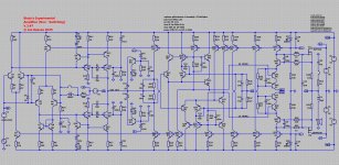
BEANS Circuit Description
Power Delivery
Power rails are +-32V volts for the MOSFETs (V4,V5). This seems to give plenty of headroom for driving +-28.3V into the speaker to give 50W at 8 ohms or even 100W at 4 ohms. Probably it could be a bit less, maybe 30V if the clamp circuitry is carefully optimised.
Additional rails are provided by V6 and V7. They extend 12V beyond the power rails. I did have them at 8V for a while but there were some issues with MOSFET drive in extreme situations so I reverted to 12V.
The amplifier uses current sources extensively. Bias for these is provided by green LEDs D17 and D18, operating at about 2V, as suggested by Cordell. The idea is that the temperature coefficient for the LEDs counters that of the current source BJTs. Also it gives a nice indication that the power rails are working if those LEDs are brought out to the front panel. Current for the LEDs is provided by R44 and R45. Those could be replaced by a single resistor, but then the LEDs wouldn't show the health of both supply rails.
Front End
Input stage.
V1 represents the source. This should be the low-impedance output of an op-amp at the end of a pre-amp which likely provides variable gain with a volume control, input filtering etc.
V2 is a voltage to eliminate output voltage offset. If you modify the circuit you might have to change this value to achieve 0V at the output. In reality, this could be a servo. There is a feedback capacitor C1 to use instead, but in most of the testing I just leave this shorted out for convenience.
Diodes D1, D2 provide input protection from excessive differential voltages. Probably more diodes need to be sprinkled over the circuit for more protection. Some circuits have diodes between the LTP collectors, but I found these limited the slew rate so I just omitted them for now.
The input goes to two differential amplifiers which drive each half of a push-pull VAS. These are biassed via current sources Q3 and Q4 which set the tail currents at about 5mA. I experimented with the emitter degeneration values (R2, R3, R6, R7) and 47 ohms seems to give good distortion levels. Feedback from the amplifier output is provided by R13 and R10 for a gain of 20. L1 is a simulation hack to test open loop gain response (it cuts AC feedback while allowing a DC path). C1 is the normal feedback capacitor to set unity gain at DC to reduce output offset. V3 is another hack to test loop response for establishing gain and phase margins.
The bottom LTP (Q5, Q6) has a current mirror (Q7, Q8). Testing showed this improves performance as expected. Upgrading to a Wilson mirror or more complex varieties didn't show any improvement.
The top LTP (Q1, Q2) doesn't have a current mirror. This is because that having mirrors in both places leads to a current indeterminacy where there is nothing programming the quiescent current through the VAS and it ends up being pot luck what current you get there. Here, approximately 2.5mA is flowing through R1, setting a voltage which propagates through Q11 and Q13 to set the VAS current at R11.
I tested putting the current mirror at top vs. bottom, and it seemed much better at the bottom. This might be expected due to the better performance of NPNs.
VAS
The VAS is a push-pull configuration. I did briefly try a single-ended design with a current source but distortion was worse and slew rates were asymmetrical. With more application, a single-ended VAS might be as good or even better though. But I liked the look of the push-pull topology so I stuck with it.
Outputs from the LTPs are buffered by emitter followers Q11, Q12 into loads R11 and R15. R12 and R14 limit the current in case of disaster.
Q13, Q16 are the VAS transistors and provide the gain. Their emitter degenerators R16, R17 are intentionally quite high so that the VAS current can be reliably programmed by R1. VAS overload protection is provided by Q9, Q10 and D3-D6. If the base of Q13 or Q16 exceeds a certain value, these conduct, clamping the drive to the VAS. LEDs D3 and D6 could be at the front panel to show the overload state for nerds. In fact you can omit Q9 and Q10 and just use LEDs to clamp the VAS input, but the circuit as shown gave a better response, and keeps the potentially noisy LEDs away from the signal path in normal circumstances.
Q14, Q15 are cascodes for the VAS transistors. These reduce distortion by about a factor of 2. D7 and D8 prevent cascode latch up, which will occur if the bases of Q11 or Q12 exceed the cascode bias voltage by more than about 2 Vbe's. When this happens, current through the VAS falls to nearly zero and stays there. Cascode biassing is provided by the 5.1V zeners D9, D10 which are in turn biassed by R18, R19 and decoupled by C4, C5.
Dominant pole compensation is effected by Miller capacitors C2 and C3. C3 is roughly twice the size because, (if I understand correctly) the closed loop gain of the lower input stage is double that of the top, and the Cdom's need to match.
Output stage
Clamp
Technically speaking, I believe this should be called a clipper, not a clamp. But everyone seems to call such circuits clamps, and I know my place.
Testing showed that the output stage would go crazy with excessive inputs, causing both MOSFETs to turn hard on. This, children, is bad. It seems that the MOSFET bias setting circuitry (Q21-Q40) goes into foldover mode or something. I spent about two minutes melting my brain, trying to figure out a solution before deciding just to prevent excessive inputs in the first place. First I tried a diode clamp. It was fine, but a little soft in its response, and also needs quite a hefty standing current. So I devised the circuit as shown.
Zeners D15, D16 provide a reference voltage near to the power rails, biassed by R20, R21 and decoupled by C8, C9. If the input gets too close to that point common-base transistors Q17 or Q18 conduct, dumping current through LEDs D13 or D14. Note that the maximum output current from the VAS is around 20mA, so that suits the LEDs nicely. I know what you nerds are thinking, and you are correct. Also, you might think the decoupling capacitors C8, C9 aren't necessary as the zeners aren't normally in the signal path. But without them, the amplifier oscillates during clipping for some reason. D15 and D16 protect the transistors from excessive negative voltages.
Output stage biassing
In order to achieve the non-switching behaviour, the current through each MOSFET must naturally stay positive at all times. This is what distinguishes a non-switching amplifier from a class-B or AB one. The circuit which accomplishes this is quite complex, Q21-Q40. It's symmetrical, so for brevity I'll just describe the high-side.
This design achieves always-non-zero-current-through-the-MOSFET-ness by ensuring that the small voltage across R50 is kept positive. This feat is essentially accomplished by the active clipper circuit formed by Q22 and Q25. An active clipper is needed because the output voltage has to be controlled very precisely. The output at the emitters of these transistors follows the higher of the two base voltages, one being the input voltage (more or less) and the other being a small voltage higher than the amplifier output voltage. Basically this "small voltage" is the minimum voltage that can exist across R50. Q22 and Q25 are cascoded by Q21, Q24. This is desirable to avoid changes in bias due to the Early effect. Without the cascoding, the current through the 'inactive' MOSFET sags during its minima. C10 and C12 were derived empirically to avoid a nasty pole at around 80MHz. The amplifier is still normally stable without them though.
The output of this 'minimum clipper' is buffered by emitter follower Q33, and is then delivered to the MOSFET driver stage. The bias for the cascodes Q21, Q24 is taken relative to this point, and provided by R29, current source Q29 and is decoupled by C11. The emitter follower itself is also cascoded by Q32 which uses the same bias point. It might seem like overkill to cascode emitter followers in this way but they are dealing with a large voltage swing and need to be precise to within millivolts, so it makes a big difference to performance.
The voltage from the VAS that is input to the 'minimum clippers' should be offset for best performance. This is done by R23,R24 and current sources Q19, Q20. It turns out that a slightly negative offset is needed, which is why the wires are crossed after this network. In practice, adjusting R23 and R24 control the point at which the MOSFET currents cross-over, i.e. this sets the quiescent current of the output.
In simulation, R23 and R24 have been the same, so maybe in a built amplifier they could be replaced by a single pot. C6 and C7 are necessary bypass caps so that HF response isn't affected by the resistors.
The reference voltage supplied to the 'minimum clipper' and fed to the base of Q25 is created by R36 and associated current sources Q39, Q40. Again it's bypassed by C14. Decreasing this resistance increases the minimum current in M1. R36 needs to be carefully adjusted to get the correct minimum output current. Due to the vagaries of component variation, each side needs its own pot. The network as shown is likely the simplest, but there may be more technician-friendly ways to arrange the bias adjustment, like having pots for spread and offset instead of adjusting each side separately. Also because of component variations it may be that a different arrangement is needed that can accommodate both positive and negative bias adjustments. Probably I would do that for a prototype build, just in case.
Drivers and output
So now, we have two output-level signals (marked as HI_DRIVE and LO_DRIVE on the schematic) which are applied to the MOSFET drivers through PNP followers Q44 and Q48.
I think my way of driving the MOSFETs might be original. Each MOSFET acts as a voltage follower which is linearised by an associated transistor (Q44,Q49). I think of these transistors as operating in common-base mode, with the bases referenced to the sources of the MOSFETs. This way the output at the drain is just one Vbe away from the drive signal.
This gives local gain, greatly increasing the effective gm of the MOSFET, and removing the annoying variability of the threshold voltage. And because is common-base, it's nice and fast (gate capacitance excepted). Q43 provides the pull-up for the gate. R46, R47 and C18 are for stability. I adjusted these without doing 'hard sums' but by looking at Bode plots and square waves. Q46 is another cascode, again to help with sagging at the current minima, biassed by R40, Q42 and decoupled by C16.
Each MOSFET drives the loudspeaker through source / sense resistors R50, R51. I chose 0.1 ohm for these when I started out, and haven't found any reason to increase them.
C23 and R52 are the Zobel network, just to ensure the amplifier is loaded at high frequencies if, for example, the speaker is disconnected. L2 enhances stability HF performance by isolating the amplifier from capacitive loads, probably caused mostly by loudspeaker cables.
The speaker is just a resistor with some lines drawn next to it. I didn't make a loudspeaker equivalent model or anything.
That's it! Thanks for reading! If, after following my directions, you get lost, just come back here and I'll tell you again.
Haha. I guess! I prefer to keep things simple but maybe I'm not clever enough to figure out a simple way of doing it. I am working on a simpler amp though!Nice piece of Maximalism. 😎
As promised, here's some pics.
Output is in red, blue and green traces show the currents thru the MOSFETs. Notice the currents don't go to zero and there is a nice smooth transition. Input 1kHz, 1.414V peak. Output 50W into 8ohms:

Here's a zoomed image, you can see the currents 'sagging' a little at the bottom. I think this is mostly due to the Early effect:

A sine wave clipping. Input 2V peak, 1kHz:

There's a little bit of sticking as it comes out of clipping. I'm still trying to solve that little problem. Here's a close up:

Here's a 20kHz sine. 1.414V input, 50W output:

And a close up of the bottoms. You can see a bit more sagging and irregularity:

Output is in red, blue and green traces show the currents thru the MOSFETs. Notice the currents don't go to zero and there is a nice smooth transition. Input 1kHz, 1.414V peak. Output 50W into 8ohms:
Here's a zoomed image, you can see the currents 'sagging' a little at the bottom. I think this is mostly due to the Early effect:
A sine wave clipping. Input 2V peak, 1kHz:
There's a little bit of sticking as it comes out of clipping. I'm still trying to solve that little problem. Here's a close up:
Here's a 20kHz sine. 1.414V input, 50W output:
And a close up of the bottoms. You can see a bit more sagging and irregularity:
This is what a square wave looks like. Input 1V pk, 10kHz, 10nS rise and fall times. Output is 20V peak, 8 ohms:

As you can see there's a little bit of overshoot. This can be fixed by increasing Cdom, but of course it's a compromise. I think this is okay.
Here's a close up of an edge. The edges are very similar and symmetrical so I'll just show this one as typical:

Here's the closed-loop gain plot. -3dB comes in about 3MHz:

And open-loop gain. P1 @ 2Hz, open-loop gain 143.9 dB, unity gain bandwidth 17MHz.

Finally, loop gain showing phase margin of 64.7 degrees and gain margin of 12.95dB:

As you can see there's a little bit of overshoot. This can be fixed by increasing Cdom, but of course it's a compromise. I think this is okay.
Here's a close up of an edge. The edges are very similar and symmetrical so I'll just show this one as typical:
Here's the closed-loop gain plot. -3dB comes in about 3MHz:
And open-loop gain. P1 @ 2Hz, open-loop gain 143.9 dB, unity gain bandwidth 17MHz.
Finally, loop gain showing phase margin of 64.7 degrees and gain margin of 12.95dB:
In my description I forgot to mention the function of C22. It's too late to go back and edit. In early versions of the amplifier, there was a problem with square waves, where both MOSFETs would turn on together. Instead of playing a nice game of push-me-pull-you they wanted a tug-of-war, resulting in peaks of up to 50A. Part of the solution lay in C22, which fixes this with very few downsides. If one MOSFET suddenly feels the need to turn on due to rapidly rising gate voltage, this will pull down (off?) the other MOSFET, and vice-versa. This effect only really happens with fast transitions, so doesn't significantly affect normal operation or biassing.
Here's a pic of current transfer during a fast edge, 1V pk input, 10nS:

Here's a pic of current transfer during a fast edge, 1V pk input, 10nS:
Have you run the FFT without the non switching function? I'm a fan of the concept but every manufacturer who has had it moved on to other topologies. Not sure if it was for economic or performance reasons.
The complexity of this design make me wonder if it was economic. Although I should point out that all the BEANS components are easily available, low-cost, off-the-shelf parts.Not sure if it was for economic or performance reasons.
- Home
- Amplifiers
- Solid State
- B.E.A.N.S. Amplifier