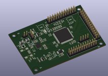
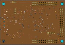
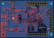
Hi, here is a first draft of the board. 4 layers: Signal / GND / GND / Signal+Power. There is room for improvements for sure.
Still looking how to manage the shielding of the USB receptacle.
Comments welcomed 🙂
KiCAD files here
JMF
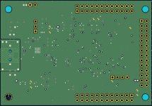
Still looking how to manage the shielding of the USB receptacle.
Comments welcomed 🙂
KiCAD files here
JMF
Attachments
Quite impressive! Will it work with UAC2 on Linux? I wonder why you dont have isolated outputs, especially on the clocks and i2s lines. Earlier in this thread, I gathered this was a good thing to have. I think the STM32 may cause quite a lot of noise that would go into the DAC ground.
The programmed device should be seen as a USB 2.0 HS UAC2 device on all OS (Linux, Windows...)
As developped above, top performance seem achievable without isolation. It was advised to keep things simple to start. I started by putting some noise filtering at USB receptacle level. many top performing devices don't have isolation between DAC and surrounding devices. Let's see what we will achieve here.
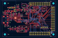
I still have things on the todo list:
As developped above, top performance seem achievable without isolation. It was advised to keep things simple to start. I started by putting some noise filtering at USB receptacle level. many top performing devices don't have isolation between DAC and surrounding devices. Let's see what we will achieve here.
I still have things on the todo list:
- adjust track width for impedance matching where needed,
- add GND vias near high speed tracks changing layers,
- USB shield management (don't know how to do it well),
- Is PCB for the Oscillators OK?
- check if more elegant routing of tracks is possible,
- Tiddy things...
If you are using USB-C the specification mandates that shield is connected to ground at both ends of cables. So board connector shield should be connected to ground as well. Same works well with older USB connector types as well.USB shield management (don't know how to do it well),
Hello, I'm using USB-mini. If I understand well, the USB receptacle shield should be connected to the chassis and "Earth", and connected to the board GND through R//C.
I wonder if I can leave the GND plane below the USB connector, Or if it would be better to remove GND plane below and have instead a "Shield" area below the connector with hole to allow connection to the chassis.
I also wonder if I need to ajust the D+/D- track to have them of equal length.
JMF
I wonder if I can leave the GND plane below the USB connector, Or if it would be better to remove GND plane below and have instead a "Shield" area below the connector with hole to allow connection to the chassis.
I also wonder if I need to ajust the D+/D- track to have them of equal length.
JMF
Wondering if it would be possible to use the USB-C connector - USB Mini B has been around for a really long time now, and the cables for that are getting harder to find. It is fairly easy to integrate USB-C connector and they are widely available on JLC PCB etc.
As for the USB connector, most devices I've seen connect the connector directly to the ground plane of the board, which is usually poured around the connector area as well. It's likely got something to do with mechanical strength as well tbh.
Thanks for creating this project - I spent a long time looking for a simple and inexpensive multi channel USB to I2S solution for active crossover speakers and it seems like there are very few of these.
Hi, and thanks for confirming that there was a niche for this project. For the connector, we had already discussed it some time ago. Based on advices here, I had discarded the micro-B and went to the mini-B as in Bohrok2610 project. A very frequent one is the "big type B". Most common today from cables perspective is type C because of phones. Have to think about it...
It seems a good practice to connect the shield to the board ground with R//C network, and not directly to the ground. I'm not at ease with chassis GND (earth) and board GND. Does it makes sense to have one of the board corner fixing holes dedicated to the chassis GND, connected to the Shield, in turn connected to the board GND through the R//C network?
I have to re-read:
https://www.eevblog.com/forum/projects/usb-shield-ground-connection/
https://electronics.stackexchange.c...t-a-usb-shield-on-a-pcb#comment1270229_498039
The particular niche for this project is actually quite underserved. Most SBCs outside of RasPi have undocumented I2S capability, and RPi before 5 only have two channels of I2S. For RPi5, the HiFiBerry DAC8x exists, but the MCHStreamer (105USD) and the DIYINHK multichannel XMOS thing (69USD) are the only real alternatives outside of professional audio interfaces for USB-multichannel I2S. CamillaDSP seems to be a good choice, and after wasting too much time on ADAU boards that didn't work, it seems to be a nice modular solution for building general audio projects around.
Seems like there hasn't been a lot of buzz in the software channel lately; would you say the software side of this is relatively close to being complete (initially, anyway?)
I think that in many USB cables, there is no real distinction between ground and shield, particularly for higher-current charging cables. I've definitely seen many where the shield is used with a bare ground wire, probably to increase current carrying capacity without increasing the thickness. At best, having the connector shell indirectly connected would be a cable dependent situation.
My suggestion is to move to USB-C and forget about the R||C network as that is useless with USB-C. Actually I doubt if it is really needed with any type of USB connector in a board like this.
Thanks for the feedback bohrok2610.
Because I don't install Isolation devices, I wanted to filter as much as possible noise coming from the USB at USB level. Hence several not mandatory features included:
Sure that if isolators are implemented, all the above is much less important.
But OK to move to USB-C receptacle to be future proof.
Because I don't install Isolation devices, I wanted to filter as much as possible noise coming from the USB at USB level. Hence several not mandatory features included:
- ferrite beads on VBus,
- common mode choque on data lines,
- decoupling of shield from GND with R//C network...
Sure that if isolators are implemented, all the above is much less important.
But OK to move to USB-C receptacle to be future proof.
DAC8x are just 4 PCM1502A chips places onto one PCB. IMO very similar results would be with using 4 PCM1502A boards from Ali, each for 1.5USD. Also the MCLK is available, when the GPCLK gets working, unlike on DAC8xFor RPi5, the HiFiBerry DAC8x exists
This is the 2024 hobby project but there time competition with high professional workload and some outdoor activities (Wingfoil especially). Software proof of concept demonstrated feasibility, but I couldn't go much further with the discovery board I have. So I switched to the hardware part.
For software, a choice will have to be made between the classic stm32 stack (which I don't like that much) or ThreadX /UsbX one which is not yet complete for the sampling rates end bit depth config.
So still some work on the software part.
For software, a choice will have to be made between the classic stm32 stack (which I don't like that much) or ThreadX /UsbX one which is not yet complete for the sampling rates end bit depth config.
So still some work on the software part.
Here's a couple of Application Notes from Würth which I found useful:Thanks for the feedback bohrok2610.
Because I don't install Isolation devices, I wanted to filter as much as possible noise coming from the USB at USB level. Hence several not mandatory features included:
- ferrite beads on VBus,
- common mode choque on data lines,
- decoupling of shield from GND with R//C network...
Sure that if isolators are implemented, all the above is much less important.
But OK to move to USB-C receptacle to be future proof.
ANP002 The Protection of USB 2.0 Applications
ANP024 The USB Interface from EMC Point of View
After investigation, by spec, the Usb-C Gnd and shield are connected (thanks bohrok for the information). I really liked the idea to protect the board a bit from Usb noise. Shield decoupling was a part of that. I won't be able to measure the impact of doing it or not.... I have difficulty to discard it :-(
I'm travelling, so not much time to stick in front of the computer for details. After some decantation, I'll keep the shield with some separation from the board ground. This discards the USB-C option. I was about to switch to the big type A, but then remembered the elegant stacking of bohrok DAC. This is a good option to avoid flat cables. A "slim" connector is nice in this configuration. So I will stick with the mini USB profile (micro usb not being a good option, Usb-C discarded because of the above).
Should I keep or remove the GND plane below the oscillators pattern?
https://ecsxtal.com/crystal-and-oscillator-printed-circuit-board-design-considerations/ indicates for Crystals "Do not lay out the ground (GND) pattern under crystal unit, this adds parasitic capacitance" but I don't know if this applies to Oscillators.
https://www.byte-lab.com/best-practices-for-crystal-oscillator-layout-2-3/ indicates what I understand to be the contrary "In most of the cases, there is no need for any GND isolations. ... If you are on a multi-layer PCB, simply ensure you have a clean GND plane between the oscillator and other traces.
How to you proceed?
JMF
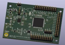
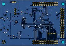
Spent some time to finalize the PCB:
- adjust track width for impedance matching where needed,
- add GND vias near high speed tracks changing layers,
- USB shield management,
- checked footprints,
- Improve GND plane by spacing vias to minimize islands,
- Silkscreen.
Attachments
If you are using USB-C the specification mandates that shield is connected to ground at both ends of cables. So board connector shield should be connected to ground as well. Same works well with older USB connector types as well.
It is always funny and kind of shocking that there is always disagreement over shielding. In the app node of the USB3300 IC, they say the "industry convention is to only ground the host side of the cable shield". I wish they could point to where this convention is written down! I have not read the USB-C spec. but it would be good to read what they say too.
However, what is written in the app note makes perfect sense to me and is what I do: with a connection at one end (host) the shield becomes an extension of the host's chassis, protecting the data wires from EMI. By not connecting it to the host, noise currents cannot flow in the boards ground, and it also eliminates current ground loop current flow caused by the host and device being at different potentials.

See e.g. latest USB-C specification chapter 3.4.2 USB 2.0 Type-C Cable Assembly. Table 3-11 USB 2.0 Type-C Standard Cable Assembly Wiring states this in note 6:I have not read the USB-C spec. but it would be good to read what they say too.
6. Shield and GND grounds shall be connected within the USB Type-C plug on both ends of the cable assembly.
- Home
- Source & Line
- Digital Line Level
- STM32 USB to I2S multi channel - Hardware part