Hi Mooly, As I think about this more, isn't Q4 more important than Q5? With the beta-enhanced VAS, I thought the specs of the second transistor (Q5) aren't as important. Isn't it Q4 that has the larger influence?
Yes up to a point, and Q4 has it easy in terms of dissipation but if you hang a slower high power device in there in place of Q5 then that is still a limiting factor.

As your at the design stage, have you considered using solid-state relays (MOSFETs)? Its now widely held that relays won't definitely protect under all failure conditions as they can arc and become welded closed.
Yes, I know the mosfet system for speaker protection well.
At the moment I prefer to use high power relays. I usually use the T90 model of 30A rms.
In the future is possible...
At the moment I prefer to use high power relays. I usually use the T90 model of 30A rms.
In the future is possible...

Hi Guys
i need help
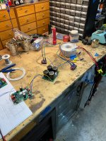
i tried to power up my pcb. it is my first AMP with DC servo.
rail 32V
R27 st to 10K // 10k under the pcb to get more power for the Zener with 32v rail.
no TL071 and MOSFET inside. extra cable(green cable from Input GND to power GND, input shorted
R26-Output resistor is not inside..maybe i will use sadface output PCB
measurements:
R channel, L channel nearly the same
R5 586mV that is about 5mA on the CCS....ok
PIN 4 -11,95V..........................................................ok
PIN 2 6,46V ?
junction R19/R20 7,13V?
PIN 6 2,13V...?
500R poti is not reacting when i try 6 turns right/left? i re check the soldering
thank you
chris
i need help
i tried to power up my pcb. it is my first AMP with DC servo.
rail 32V
R27 st to 10K // 10k under the pcb to get more power for the Zener with 32v rail.
no TL071 and MOSFET inside. extra cable(green cable from Input GND to power GND, input shorted
R26-Output resistor is not inside..maybe i will use sadface output PCB
measurements:
R channel, L channel nearly the same
R5 586mV that is about 5mA on the CCS....ok
PIN 4 -11,95V..........................................................ok
PIN 2 6,46V ?
junction R19/R20 7,13V?
PIN 6 2,13V...?
500R poti is not reacting when i try 6 turns right/left? i re check the soldering
thank you
chris
Attachments
Last edited:
You must have the opamp fitted as that provides the required DC bias for the input stage.
No opamp means the base of the input transistor is floating at DC and will be biased purely by leakage through the input coupling cap.
No opamp means the base of the input transistor is floating at DC and will be biased purely by leakage through the input coupling cap.
Hi Mooly
Mooly amp :
ok with DC OPV it is working. (embarrassing DC servo amp without opamp 😆)
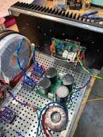
no lateral MOSEFT soldered. 31V rail
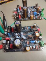
R channel / L channel
PIN 6 -487 / -4,98V
PIN4 -11,92V / -11,69V
DC offset both 0V
R5 - CCS 590mV / 586mV ---> 5,9mA / 5,86mA...perfect
with trim pot is set both channels to:
R20 582mV - 26,45mA
R19 625mV - 28,4mA
Q1 :not possible to get this the same - okay?
Q2: which Voltage should i measure to be "right" for the voltage on the gates of the MOSFET?
i mean collector to GND T6 / T7
kr
chris
Mooly amp :
ok with DC OPV it is working. (embarrassing DC servo amp without opamp 😆)
no lateral MOSEFT soldered. 31V rail
R channel / L channel
PIN 6 -487 / -4,98V
PIN4 -11,92V / -11,69V
DC offset both 0V
R5 - CCS 590mV / 586mV ---> 5,9mA / 5,86mA...perfect
with trim pot is set both channels to:
R20 582mV - 26,45mA
R19 625mV - 28,4mA
Q1 :not possible to get this the same - okay?
Q2: which Voltage should i measure to be "right" for the voltage on the gates of the MOSFET?
i mean collector to GND T6 / T7
kr
chris
Last edited:
typo !!! above.......sorry
with trim pot is set both channels to:
R20 582mV - 2,645mA
R19 625mV - 2,84mA
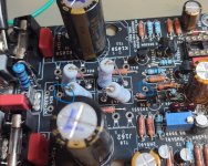
driver BJT T6 /T7
R17 4,23V, T6 Vce 26,1V
R22 3,94V, T7 Vce 26,5V
both channel exact the same.
So for T7 i got power dissipation of Vce 26,5* 0,002645A = 70mWatt...check!
is that enough current for 2x Lateral MOSFET gate charge?
kr
chris
with trim pot is set both channels to:
R20 582mV - 2,645mA
R19 625mV - 2,84mA
driver BJT T6 /T7
R17 4,23V, T6 Vce 26,1V
R22 3,94V, T7 Vce 26,5V
both channel exact the same.
So for T7 i got power dissipation of Vce 26,5* 0,002645A = 70mWatt...check!
is that enough current for 2x Lateral MOSFET gate charge?
kr
chris
With FET's removed and with the bias pot set to zero ohms (a short) there should still be zero volts offset at the output and the gate connection to each missing FET should be very close to the rail voltages. There should be almost zero current in the 1k5 resistors (so no volt drop across them).
With the bias turned the other way you shpuld see voltage develop across each 1k5. A 500 ohm preset should get you around 4 volts across each 1k5 resistor. Turn the preset back to no bias again before fitting the FET's
With the bias turned the other way you shpuld see voltage develop across each 1k5. A 500 ohm preset should get you around 4 volts across each 1k5 resistor. Turn the preset back to no bias again before fitting the FET's
Hi Mooly
okay, not fully clear for me but i will do so.
so i understand that it is not possible to make a pre setup before solder in the MOSFET´s.
thx
chris
okay, not fully clear for me but i will do so.
so i understand that it is not possible to make a pre setup before solder in the MOSFET´s.
thx
chris

- Home
- Amplifiers
- Solid State
- My MOSFET amplifier designed for music