Marcel,
is trying to force simulated spikes in the information stream not looking in the wrong direction.
What exactly is the difference when the .dsf file is made with a quasi multibit converter (QMC) instead of with a one bit PCM2DSD .
Mostly the spectral shape of the out-of-band stuff: just huge noise (my quasi-multibit algorithms, presumably HQPlayer's as well) or somewhat smaller but still huge noise and FM-like tones and their aliases around fs/2.
Isn’t that difference the amount of HF noise that is quite a bit lower with the QMC ?
I think it is somewhat larger, actually.
When you interpret a high level as +1 and a low level as -1, the mean-square value of a bit stream (what signal theorists call power) is independent of the data. As the power of the desired signal is essentially the same and the quasi-multibit converter doesn't produce the big peaks around fs/2 that a normal sigma-delta modulator produces, there must be more power left for (HF) quantization noise.
When being processed by the Firdac’s shift registers, both versions will have to deal with the same spike problem, but after being filtered the QMC version doesn’t show the odd spectral lines caused by FM.
So seemingly not the spikes but the larger HF noise are causing this.
Should therefore not all the attention being given to the reconstruction filter instead of looking at spikes produced by the shiftregisters?
Hans
See my report (pdf file attached to post #2696) for my point of view. I think it's intermodulation between the tones around fs/2 that is apparently generated in the output filter, even though those tones are suppressed substantially by the FIRDAC and the 8.2 nF capacitors.
When you look at the spectrum plot with a simple single-bit sigma-delta and an offset in post #2696, you see a peak greater than 0 dB DSD around 2.8174 MHz. Its alias around 2.8274 MHz is equally large and the first op-amp stage in the filter has quite limited loop gain at such frequencies. Still, the intermodulation products bohrok2610 measured are only about -130 dB DSD.
Last edited:
I still have to have a look at their source code. Highly effective dither scheme perhaps?As I showed in post #2667 there are also simple 1-bit modulators that do not show spectral lines with this DAC. So same digital path, same shift registers, same output stage but different 1-bit modulators. One causes spikes, the other doesn't.
To illustrate the difference in out-of-band spectra, I've dug up a few old plots for the sigma-delta modulator algorithms of my valve DAC, simulated at 28.224 MHz with just a DC offset at the input. Horizontal scale in kHz, while on the vertical scale, 0.5 corresponds to 0 dB DSD and 0.05 to -20 dB DSD. The plots don't go above 14.112 MHz, but everything aliases above 14.112 MHz, of course.
Red: PWM4 quasi-multibit
Green: PWM8 quasi-multibit
Blue: very chaotic single-bit modulator
(One of the 0 to 14.112 MHz plots is without the chaotic modulator, so you can see the others better.)
Although the chaos reduces the tones around 14.112 MHz substantially (they are not nearly as high as the 2.8174 MHz tone of post #2696), the tone below 14.112 MHz is clearly visible for the single-bit modulator (and the one just above 14.112 MHz is out of the range of the plot). For the other modulators, I don't see any obvious tones.
Apologies for the poor resolution of the pictures.
Last edited:
I think I did choose the wrong FIRDAC imperfection,.though. A difference between rising and falling delays that is the same for each flip-flop should result in data-independent common-mode spikes rather than in the worsened suppression around fs/2 that I hoped for.
Last edited:
If that's the case, presume we'll just have to see what we can do about it. We've come this far in a fascinating and educational thread so we should continue to see it through as best we can.
Besides, noise in modern dacs is a ubiquitous issue. Anything we come up with may be helpful in the future.
Besides, noise in modern dacs is a ubiquitous issue. Anything we come up with may be helpful in the future.
For the case of the DSD128 .dsf file with only an offset, the suppression of the FIRDAC is limited to theoretically 55.0176 dB by the fact that the tones are 5 kHz below and above the notch at 2.8224 MHz.
Wild guess for the effect of resistor tolerances:
suppose 0.5 % tolerance resistors have independent Gaussian distributed resistance variations with 0.1 % standard deviation. There are 16 resistors contributing to the differential output signal of each DAC core, if one of them is off by 0.1 %, it presumably reduces the depth of the notch to about 1/16 of 0.001. With 16 resistors varying independently, the depth of the notch would then be limited to 0.00025 (-72 dB) in the one sigma case, 0.0005 (-66 dB) 2 sigma. This actually has less impact than the fact that the tones around half the sample rate are not exactly in the notch.
The integrator of the first stage doesn't integrate much at 2.8 MHz. Assuming that the output impedance of the op-amp is still low, the 8.2 nF capacitors are essentially connected to nodes with a resistance of about 130 ohm to ground. 1/(2π 2.8224 MHz 130 ohm 8.2 nF) ~= 0.0528986, or -25.53111 dB.
All in all, tones 5 kHz above and below half the sample rate of DSD128 will ideally be suppressed by about 80 dB by the FIRDAC and 8.2 nF capacitors together. Resistor tolerances are unlikely to affect this much, although they could have a substantial impact at smaller frequency offsets and higher DSD rates.
No idea what effect other imperfections have.
I assume by analogue input filtering you refer to filtering after conversion (before opamp input) which I would call output filtering. IMO that is filtering after the damage has already been done. Digital filtering before the dac makes much more sense as it removes large chunk of out-of-band noise before conversion takes place.Yes, I agree, input filtering makes all the difference, either digital or analogue.
Last edited:

IME, that causes more noise problems than if bypass currents are kept more on the surface layer. A decision was made to route the shift register signals on the surface, and to duck the bypass currents down through a lower layer. I'm not sure what would happen if the opposite strategy had been used, which would be to use solid surface fill under the shift register chip as a low inductance bypass current path. To do that would require ducking all the data signals down through a lower layer. Which approach would be worse in terms of shift register output noise?
I agree. It is best to keep a common ground plane on top.
What is more, all signals are best routed impedance controlled on a layer between GND and Vcc. Why?
This is both a CMOS output and a CMOS input.
The input capacitance (Ciss) of the P-Channel input is linked to Vcc while the input capacitance of the N-Channel is linked to "GND" (remember, Ground isn't)
So with any transition one of these capacitors is charged while the other is discharged.
We all learn that in PCB Layout any high frequency signal trace should be matched with "Ground", which commonly these days is a ground plane.
BUT, for the P-Channel device actual "Ground" is Vcc and "Ground" is actually it's Vcc.
Thus in CMOS VCC and VSS should be treated equally. What amazes me that this was all in Ott's tome decades ago.
Given the need for a signal plane between VCC and VSS it is often best to use 6 or 8 layer PCB's, yes they cost more, 8 layer is double of 4 layer, however we now have enough layers for planes and buried strip lines for all signals.
In mixed signal designs I commonly make sure to completely separate analogue (+/-5...18V etc.) sections from digital with one ground plane being common to everything.
Top is commonly flooded with ground fill, then a Vcc Plane then signal, then main ground plane then the second Signal routing plane and then second Vcc (I often have systems where 1.2..1.8V drive IC cores at relatively high currents and 3.3V are just I/O voltages and logic sections of DAC IC's etc.) then another signal layer and and finally another ground fill on the bottom.
I often locate bypass capacitors directly under the IC being "bypassed" and I use three vias around each pad to reduce via impedance.
Yes, an 8-layer PCB with components on both sides roughly doubles the cost of PCB and assembly of PCB, but for quality audio the contribution of these elements compared to the rest of the BOM are moderate.
Ultimately the way I now look at PCB's is to ask "how are current loops closed" and design based on that. Power supplies and ground I simply all consider as signal returns.
The above having been said, don't know offhand which strategy would be best/worst in the end. Again, its just that IME there can be considerable benefit to keeping bypass currents on the surface layer through a direct path.
For classic CMOS IC's with pin 7/8 GND and pin 14/16 VCC I found best is GND and VCC Plane and bypass capacitor under the IC with generous use Via's, or better four identical capacitors in the four corners of the IC on top. I now use only 1uF/25V/X7R/0603 for logic bypass, others only if mandated by manufacturer. and then usually 10nF or smaller.
It may seem counter productive but using just one value of capacitors and many together with solid Vcc and Vss planes delivers very low noise (again, it's all in Ott's tome).
As a rule, I try to avoid classic CMOS (actually TTL 74 class) layout IC's completely and either use popcorn logic (mostly NC7SZ Tiny Logic from Fairchjld/On) or 16 Bit parts which have much better layout of GND and Vcc Pins.
There are four VCC Pin's and 8 GND Pins and the logical bypass layout has 8pcs of 1uF 0603 topside as close to the pin's as PCBA allows. This gives a local bypass impedance of appx. 0.1 Ohm at 172MHz and a minimum of a hair over 0.001 Ohm at 5MHz. I'd a pair of big value (say 470uF) electrolytics to either side. Voila - once channel of a balanced 8 Bit FIR DAC.
Thor
It would presumably produce a common mode noise for the output stage to deal with.
That's not so much the problem as is the threshold shift on clock inputs...
Thor
The Firdac as it's name suggests is a digital Fir filter, in this case with a notch at fs/2, but with its short length, filtering is far less effective as in your AK4493.I assume by analogue input filtering you refer to filtering after conversion (before opamp input) which I would call output filtering. IMO that is filtering after the damage has already been done. Digital filtering before the dac makes much more sense as it removes large chunk of out-of-band noise before conversion takes place.
But with digital filtering you always keep all the mirrors that will have to be removed by analogue filters.
One idea to make Marcel's Firdac more effective in digital filtering , would be to change the two sets of 4 parallel shift registers into two sets of 8 registers in series, that implies just changing two connections.
This will change the first notch rom fs/2 to fs/4 and may help to cope in a better way with the HF noise.
Hans
At a DSD128 rate, that will theoretically improve the suppression of a tone 5 kHz below half the sample rate by 0.000135 dB while removing the cancellation of systematic mismatch between the flip-flops due to unequal on-chip wiring. It should make the audio noise floor somewhat less sensitive to the phase noise floor of the bit clock.
Even when both 8 shiftregisters are spread over the two chips, just as they are now ?while removing the cancellation of systematic mismatch between the flip-flops due to unequal on-chip wiring.
Hans
Yes.
The idea is that in every cycle, either U7 Q0 and U9 Q1 or U9 Q0 and U7 Q1 produce a pulse, in order to make the reference current as data-independent as possible. Adjacent flip-flops on the same chip will have relatively little random mismatch between them, much less than between chips of the same type, but there could be systematic differences between Q0 and Q1 due to different on-chip wiring. The swapped connections on the other 74LV574A are supposed to correct for that.
You will spoil that to some extent when you use the two 74LV574As as 8-tap shift registers. I can't estimate how much or how little effect that will have.
With normal 4-layer board having components on top layer the top plane is more of a pour and it becomes tricky to provide continuous impedance controlled plane for signal traces.It is best to keep a common ground plane on top.
Yes, they do cost quite a bit more. E.g. at JCLPCB Marcel's DAC board would be about 65 euros for 6-layers or 95 euros for 8-layers (5 pcbs) + shipping & taxes. All that for uncertain (or at best slim) benefits.Given the need for a signal plane between VCC and VSS it is often best to use 6 or 8 layer PCB's, yes they cost more
IME, figuring out how to make better dacs has not been a low-cost hobby. Not as bad a taking up flying planes though (as did at least one of the commercial designers in this forum).
That said, revising Marcel's 4-layer board to duck the data signals rather than the bypass currents could be tried with a 4-layer board. The "expense" would mostly in the form of labor for revising the board layout.
That said, revising Marcel's 4-layer board to duck the data signals rather than the bypass currents could be tried with a 4-layer board. The "expense" would mostly in the form of labor for revising the board layout.
Last edited:
If you feel this is important the best way for you to proceed is to revise the board layout yourself and report back your findings.That said, revising Marcel's 4-layer board to duck the data signals rather than the bypass currents could be tried with 4-layer board. The "expense" would mostly in the form of labor for revising the board layout.
Regarding Sigma-Delta streaming signal processing for FIR filtering, please see the attached. It appears to involve requantizing, which may change the sound in some unintended way. For instance, please consider all the modulators in HQ Player. Many people find they all sound different, and not all of them equally good.
Attachments
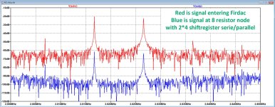
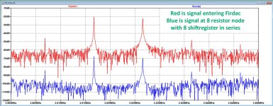
I compared 2x4 with 1x8, while using your DSD128 .dsf file with ca. 8mV offset, the output of the shift register connected to a 4th order Butt. filter.At a DSD128 rate, that will theoretically improve the suppression of a tone 5 kHz below half the sample rate by 0.000135 dB while removing the cancellation of systematic mismatch between the flip-flops due to unequal on-chip wiring. It should make the audio noise floor somewhat less sensitive to the phase noise floor of the bit clock.
For the FFT data was sampled with 1Ghz and no window function.
In the two images below, the spectrum is simulated from one of both signals entering the Firdac's shift register in red, together with the signal at the node where the 8 resistors are coming together, this output corresponding to the Firdac's input signal, in blue.
The 5Khz that you mention around fs/2 is clearly visible before and after the Firdac's shift register, but in case of 1x8, the 5Khz peaks are 6dB lower in level.
Hans
Attachments
Maybe by using weighting factors with different resistor values, transfer function could be even further improved.
Hans
Hans
- Home
- Source & Line
- Digital Line Level
- Return-to-zero shift register FIRDAC