See VR4, VR5, VR6, VR7A, but so far not seeing VR1, VR2, or VR3. Wouldn't be the first time I had trouble finding something. Maybe you could make it easy and circle it in the schematic?
While we're at it, may as well be exact about where the voltage is being measured too 🙂
While we're at it, may as well be exact about where the voltage is being measured too 🙂
Last edited:

Hi Mark,
The pot is on page 2 of 3. I had trouble finding it too.
Agree, what's being measured? Couldn't find any method for output offset error tweak.
The pot is on page 2 of 3. I had trouble finding it too.
Agree, what's being measured? Couldn't find any method for output offset error tweak.
This is an unusual design, IMHO.
There are many, many suspects for a possible out-of-tolerance part. Check bias drop across R108--- it should have the same as drop R106.
Is voltage drop across VR6 nearly 0V? Excessive wiper resistance could be a culprit.
Is the other channel biasing correctly? If so, make comparative voltage checks.
To help narrow the field of search, would you report the voltage between base of T15 and base of T17 (i.e. "spreader voltage") and the analogous spreader voltage in the other channel for comparison. Thanks!
It goes without saying, be careful for self and equipment. Insulate excess probe length with heat shrink. A slip of a probe can be catastrophic.
Good luck!
They are more or less in parallel with VR3 and VR6. The schematic symbol is a resistor with a straight diagonal line through it. RTD = Resistance Thermometer Detector
https://electronics.stackexchange.com/questions/581631/curly-symbol-in-rtd-ptc-thermistor
https://www.te.com/usa-en/products/sensors/temperature-sensors/resources/understanding-rtds.html
https://electronics.stackexchange.com/questions/581631/curly-symbol-in-rtd-ptc-thermistor
https://www.te.com/usa-en/products/sensors/temperature-sensors/resources/understanding-rtds.html
Voltage across R108 is 0.010v
Voltage between T15 and T17 base is 1.227v
I replace the port same thing.
The other channel bias is good at 80mv
Voltage between T15 and T17 base is 1.227v
I replace the port same thing.
The other channel bias is good at 80mv
If you're observing 101mV across R106, but only 10mV across R108, R106 is likely high resistance or open. Try measuring voltage drops directly on leads next to the body of the part to rule out open solder joints.
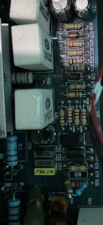
I don't understand what you're showing in post #10 pic. Looks like two series resistors?
I don't understand what you're showing in post #10 pic. Looks like two series resistors?
But the ones in question are NTC thermistors. 50 ohm, beta about 3500 - used to be common as dirt. Still got a few laying around after repairing a pair of USA1300’s that had the leads corroded off of the thermistors - Mouser 995-3DB500J. QSC still uses these in their RMX amps, and Behringer is a copy.They are more or less in parallel with VR3 and VR6. The schematic symbol is a resistor with a straight diagonal line through it. RTD = Resistance Thermometer Detector
https://electronics.stackexchange.com/questions/581631/curly-symbol-in-rtd-ptc-thermistor
https://www.te.com/usa-en/products/sensors/temperature-sensors/resources/understanding-rtds.html
Now that I study the pic again, I see partial views of R106 and R108. I can even imagine that the lower solder joint of R106 looks suspect.
Needless to say, I'm very suspicious of R106 or its soldering.
P.S. You note high bias reading, but are the associated heatsinks hot? What's voltage across R102?
Needless to say, I'm very suspicious of R106 or its soldering.
P.S. You note high bias reading, but are the associated heatsinks hot? What's voltage across R102?
AT idle the problem channel heatsinks heats up faster than the other one.Now that I study the pic again, I see partial views of R106 and R108. I can even imagine that the lower solder joint of R106 looks suspect.
Needless to say, I'm very suspicious of R106 or its soldering.
P.S. You note high bias reading, but are the associated heatsinks hot? What's voltage across R102?
I will get voltage for R102 tomorrow.
- Home
- Amplifiers
- Solid State
- EP2500 bias