I'll start a new topic on modifying a finished amplifier.
I have an assembled version of the amplifier, which I have already modified, so this will be the second change in the circuit.
* the circuit is very simple, there are no current sources in it, initially there was no correction at all, the sound in tests is below average.
Changes were made in compensation, and some modes of the cascades were changed, it began to play much brighter and livelier, but I still think that from such an array of parts using a symmetrical topology, you can make a more practical simple amplifier with high-quality sound.
in the attachment
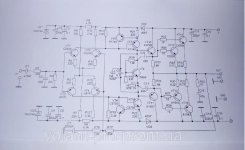
Attached is a diagram into which this block will be converted.
I have an assembled version of the amplifier, which I have already modified, so this will be the second change in the circuit.
* the circuit is very simple, there are no current sources in it, initially there was no correction at all, the sound in tests is below average.
Changes were made in compensation, and some modes of the cascades were changed, it began to play much brighter and livelier, but I still think that from such an array of parts using a symmetrical topology, you can make a more practical simple amplifier with high-quality sound.
in the attachment
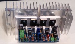
- initial diagram on a piece of paper
- photo of finished boards and cooling radiator blocks
- My power supply is standard +/-36 volts
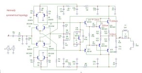
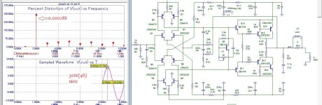
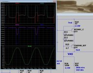
- further attached is a version of the scheme for modification, it includes the following:
- 2 pairs of differential cascades in symmetrical topology
- frequency compensation capacitor C5 (4.7pF) covers two amplification stages
- two-stage output stage
- dual output power transistors
- transistor modes were selected according to the minimal "soft" spectrum of distortion
- at a frequency of 1 kHz with an amplitude input voltage of 2 volts, distortion is less than 0.003%, at a frequency of 20 kHz - 0.03%
- slew rate 55V/µs
- output power 100 watts 4 ohms
- pole 300Hz
- open loop gain at 1kHz - 88dB (in the version on the leaflet, the open loop gain at a frequency of 1 kHz is approximately 64 dB)
- openloop unity gain frequency 3.8 MHz
Attached is a diagram into which this block will be converted.
Attachments
Last edited:
If anyone is interested in the topic, I would like to draw attention to some nuances:
1. these are resistors in the bases of the output transistors R20R21, they are scaled from 10 ohms to 47 ohms and are not divided into the bases of the dual transistor,
In the attachment in the first post on the piece of paper there is drawn an option where the base of each output transistor goes to its own 10 ohm resistor, in fact it is not logical to do this because the Q10 Q11 cascade sees the parasitic capacitance of the base through the 10ohm/2 resistor and this the capacitance is doubled, which leads to the appearance of positive feedback at frequencies above 10 MHz and a high-Q peak in the frequency response.
The model introduced input capacitances of transistors 2SK5200 and 1943, and in order to remove this sharp peak it was necessary to increase the resistor in the base and connect the bases themselves after one resistor. I think that it is more correct to parallel a pair of transistors in the implementation of a two-stage power transistor output connect the bases after one resistor.
2. Then there is compensation coil Thiel and Zobel at the amplifier output, the values fully correspond to Buche compensation equation when L2/R27=R26*C12.
With this solution, the load capacitance is permissible up to 2 μF and this will not affect the transient characteristics of the amplifier.
I think you can have DC-offset at output.
I would add some adjustment mechanism.
The amplifier is pretty simple. Even I can understand it 😀
I would add some adjustment mechanism.
The amplifier is pretty simple. Even I can understand it 😀

Thanks for the relevant question, but with the offset everything is wrong.I think you can have DC-offset at output.
I would add some adjustment mechanism.
I removed the zener diodes and removed resistors from the emitters, it was because of them that the influence of temperature on the offset and symmetry of the operating point was affected.
the circuit does not need to be balanced; 0.02 mV appears at the output and does not sense a change in the supply voltage; the difference is +/- 8 volts; there is also a slight drift 0,02V due to the influence of temperature.
With the specified initial current, the output transistors dissipate 34 watts and this does not affect the stability of the circuit parameters.
Q3 / Q5, Q1/Q7, Q2/Q8, Q4/Q6 they can be glued in pairs and you get 4 elements with 6 pins each
will further increase the reliability and stability of the circuit.
will further increase the reliability and stability of the circuit.
In the absence of current generators in the loads, 88dB of openLoop gain has already been obtainedThe amplifier is pretty simple.
those. the load of the input stages contains only linear elements.
I use this topology for very long time ago: https://anistardi.wordpress.com/2015/10/13/bass-shaker-amplifier/I'll start a new topic on modifying a finished amplifier.
I have an assembled version of the amplifier, which I have already modified, so this will be the second change in the circuit.
* the circuit is very simple, there are no current sources in it, initially there was no correction at all, the sound in tests is below average.
Changes were made in compensation, and some modes of the cascades were changed, it began to play much brighter and livelier, but I still think that from such an array of parts using a symmetrical topology, you can make a more practical simple amplifier with high-quality sound.
in the attachment
Attached is a diagram into which this block will be converted.
I agree, but the Voltage Amplifier Cascade is not a complete amplifier.Amazing low THD for low OLG + simplicity.
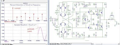
I analyzed the source of distortion in the circuit from the first post.
It turns out that the main source of distortion is the output stage in the form of a Darlington pair.
By changing the topology of the output stage, I obtained a reduction in distortion at a frequency of 20 kHz to 0.0004%, without changing the compensation parameters.
That is,
*Distortion with a 2-stage Darlington output stage at a frequency of 20 kHz is 0.03%.
*Distortion with triple output stage at 20kHz was 0.0004%.
Be careful about increasing the OLG. The fully complementary topology has two amplifiers in parallel. The tracking becomes worse with increased OLG. Add mismatch in Is between the two differential pairs and watch what happens to the second stage's idle current.
Ed
Ed
That is why I use ALL EF3... No VAS load greatly increases linearity.That is,
*Distortion with a 2-stage Darlington output stage at a frequency of 20 kHz is 0.03%.
*Distortion with triple output stage at 20kHz was 0.0004%.
Running the VAS "hotter" @ 8-10mA would greatly improve the EF2 THD. Badger is 8mA , <.01% - 20Khz . TMC drops that down to .005%...
And Tc. Thermal "creep" is inherent with symmetrical topologies. LED CCS is slightly negative Tc + this VAS is slightly positive. The use of a EF3 also allowsBe careful about increasing the OLG. The fully complementary topology has two amplifiers in parallel. The tracking becomes worse with increased OLG. Add mismatch in Is between the two differential pairs and watch what happens to the second stage's idle current.
these stages to run at lower currents. I run the VAS at <4mA (real cool). A higher OLG would push the co-efficient positive.
I have actually built many of these input stages and put the amp out on a cold winter night to --> hot room temperature while monitoring VAS dissipation.
I target <.1mA change , preferably negative.
OS
Good evening everyone.
The goal of the project is precisely the modification of the active parts existing on the board.
Because I want to get maximum performance with such a simple topology, I had to add simulate the output stage, the output stage on a 2-stage Darlington assembly does not give very good results at high frequencies.
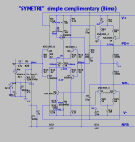
One of the possible options I am considering is converting it into a triple output stage with a “hot” Schiklai. It is composed of power transistors Q12/13/14/15 Q12/13 operate with an initial current of 46.5 mA, Q14/15 in the off state (class B),Q10/11 operate in class A.
see attachment below in this post.
From the changes:
* a progressive compensation circuit R29C2 has been added to the input to increase stability
*R5 R6 on the diagram in the first post are mistakenly indicated as 100 ohms, they are changed to 300 ohms and the current is indicated so that the mode can be checked.
*changed the value of Resistor R16 in Bias
*reduce the rating of R19 to 220 ohms for the driver Q10Q11
*reduced 22 ohm resistors in the bases of power transistors Q12Q13
*The maximum permissible load capacitance is 1 µF
in attachment - circuit and spectrum of distortion at an output power of 30 watts
The goal of the project is precisely the modification of the active parts existing on the board.
Because I want to get maximum performance with such a simple topology, I had to add simulate the output stage, the output stage on a 2-stage Darlington assembly does not give very good results at high frequencies.
One of the possible options I am considering is converting it into a triple output stage with a “hot” Schiklai. It is composed of power transistors Q12/13/14/15 Q12/13 operate with an initial current of 46.5 mA, Q14/15 in the off state (class B),Q10/11 operate in class A.
see attachment below in this post.
From the changes:
* a progressive compensation circuit R29C2 has been added to the input to increase stability
*R5 R6 on the diagram in the first post are mistakenly indicated as 100 ohms, they are changed to 300 ohms and the current is indicated so that the mode can be checked.
*changed the value of Resistor R16 in Bias
*reduce the rating of R19 to 220 ohms for the driver Q10Q11
*reduced 22 ohm resistors in the bases of power transistors Q12Q13
*The maximum permissible load capacitance is 1 µF
in attachment - circuit and spectrum of distortion at an output power of 30 watts
Attachments

Last edited:
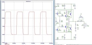
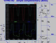
Does not clip "good" (below 1 ). 16mA pulses through the grounded pair.
Higher Ib through Q8. But no sticking ....
(below 2) is the ice cold overloaded Hawksford VAS.
If you add 6K8 resistors (R70/71) to the grounded side of the "Mod henk (symetri)" VAS , much better (below 3).
Symetri VAS....
- has local FB within the VAS , linearizing it.
-You do waste 1/2 the VAS Ic to run it.
Hawksford VAS ...
Either VAS gives about .0018% 20Khz /4R /200W , with the EF3. All these symmetrical designs have similar distortion.
The only way to get single digit of sub PPM is transitional or 2 -pole comp. w/ more OLG ("gobs" of OLG) !!
OS
Higher Ib through Q8. But no sticking ....
(below 2) is the ice cold overloaded Hawksford VAS.
If you add 6K8 resistors (R70/71) to the grounded side of the "Mod henk (symetri)" VAS , much better (below 3).
Symetri VAS....
- has local FB within the VAS , linearizing it.
-You do waste 1/2 the VAS Ic to run it.
- Symetri is the "slower VAS " @ 200V/uS. Still fast.
- 8-10mA (16-20mA total) would be the best bet to run a EF2. Low impedance VAS.
Hawksford VAS ...
- you waste 1/2 VAS Ic to run the LED's AND lose 3-4V per rail (cascode).
- Using my CFA IPS , the Hawkford can do >300V/uS ,
- OLG with the Hawksford is higher , it must have gain. But , with a higher impedance.
Either VAS gives about .0018% 20Khz /4R /200W , with the EF3. All these symmetrical designs have similar distortion.
The only way to get single digit of sub PPM is transitional or 2 -pole comp. w/ more OLG ("gobs" of OLG) !!
OS
Attachments
Having simulated many possible solutions, I settled on a real one, which improves the characteristics of the amplifier but does not require significant changes to the circuit on the board.Be careful about increasing the OLG. The fully complementary topology has two amplifiers in parallel. The tracking becomes worse with increased OLG. Add mismatch in Is between the two differential pairs and watch what happens to the second stage's idle current.
Ed
Look at the diagram attached in this post.
In fact, it turns out to only re-solder the Q3 Q8 transistor. This arrangement better stabilizes the parameters of the input pair of diff stages, this is especially noticeable with large signals.
Distortion is reduced by 3 times.
Progressive compensation R4С2/R24С8, which was done earlier, remains unchanged. The sound of an amplifier with such a compensation is better than with a multi-pole one.
Also in the circuit there are 2 power levels left for the voltage amplifier and the output stage; this solution reduces the length of higher distortion harmonics.
Attachments

R24 C8 is called shunt compensation, R4 C2 is not compensation at all, just input high pass filter.
"The sound of an amplifier with such a compensation is better than with a multi-pole one."
What is your argument to certifies that??
"The sound of an amplifier with such a compensation is better than with a multi-pole one."
What is your argument to certifies that??
Frequency-dependent parallel compensation is a first-order RC shun, "progressive" means the resistance decreases with increasing frequency. A zero order parallel shunt is linear.R24 C8 is called shunt compensation
It's nonsense to call everything just a parallel shunt.
You don’t understand the difference between a R1/C filter and R1/R4C2 compensation at the amplifier input.R4 C2 is not compensation at all, just input high pass filter.
Lots of test listening to amplifiers with different types of compensation.What is your argument to certifies that??
The distortion of the frequency response by multi-pole compensation in the negative feedback loop leads to the emergence of positive feedback at extremely high frequencies; the model does not always take into account the parasitic capacitance of the amplifier mounting design, both on the board and inside the amplifier.
Last edited:
"You don’t understand the difference between a R1/C filter and R1/RC compensation at the amplifier input."
My opinion is that you don't understand that. It is common to call compesation a network(C or RC) inside NFB loop, and R4C2 is just input filter.
Input filter influences an amp stabillity too.
My opinion is that you don't understand that. It is common to call compesation a network(C or RC) inside NFB loop, and R4C2 is just input filter.
Input filter influences an amp stabillity too.
"
Lots of test listening to amplifiers with different types of compensation.
The distortion of the frequency response by multi-pole compensation in the negative feedback loop leads to the emergence of positive feedback at extremely high frequencies; the model does not always take into account the parasitic capacitance of the amplifier mounting design, both on the board and inside the amplifier."
This not an argument good eough. Multi-pole compesation, if done well does not do that.
dadod try to use the forum elements correctly,
you distort posts in bold - teach how to format posts correctly, it’s easier than talking about compensation
Creating more imaginary poles than active gain stages reduces the stability of the amplifier circuit.
you distort posts in bold - teach how to format posts correctly, it’s easier than talking about compensation
I agree, provided that the production of ready-made amplifier boards with such compensation is established.Multi-pole compesation, if done well does not do that.
Creating more imaginary poles than active gain stages reduces the stability of the amplifier circuit.
Last edited:
It is not Darlington, strictly speaking it is emitter follower.It turns out that the main source of distortion is the output stage in the form of a Darlington pair.
- Home
- Amplifiers
- Solid State
- Modification of a simple amplifier with symmetrical topology