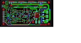
That looks better.So this is the correct way .
emitter into resistors togheter , wire for nfb, , then zobel , inductor , speaker.
You must keep the loop area of the feedback network and the input side of the LTP to a minimum. To do this, run the 0V to the front end in parallel with the feedback resistor network. Keep the front end inside side compact and loop areas between the signal hot and the 0 V as small as possible. If your board is double sided you can run the ground track to the front end under the feedback resistor.
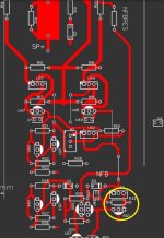
Input stage NFB is like the example (below-pink trace).... Signal ground reference should be the speaker terminal's main star point G1-speaker.
This is the final solution to get the Wolverine <1ppm/20Khz. Looping the NFB around the rails increased it to 20ppm+.
If you are just shooting for <.02-.05% "normal" distortion , you can be MUCH sloppier !
Edit ... supply grounds (G2-below) go directly to main filter cap star point.
OS
This is the final solution to get the Wolverine <1ppm/20Khz. Looping the NFB around the rails increased it to 20ppm+.
If you are just shooting for <.02-.05% "normal" distortion , you can be MUCH sloppier !
Edit ... supply grounds (G2-below) go directly to main filter cap star point.
OS
Attachments

1 or 2 or neither ?. Seeing @ostripper post , NFB there is long as well . it's about 5cm here .
Attachments
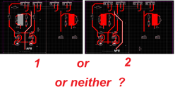
1 or 2 ? Would have to see the whole layout first. Consider that NFB is a full amplitude signal and could affect input stage traces.
On earlier "slewmaster" OP designs , I would place the 22-27K feedback resistor near the emitter resistors and run a lower level NFB
signal across sensitive input stage circuitry with a wire. A CFA amp might incur some inductive coupling.
setup that made the 30+ PPM difference (on the Wolverine). Another big improvement was to streamline the loop area(s) of the rail feeds.
Having the rails on opposite ends of the PCB (like most kits) sucks.... Stopped doing that with the post "Badger" 15 years ago.
Yes , double sided PCB's let you emulate "twisted pair" wiring right to the OP devices.
OS
On earlier "slewmaster" OP designs , I would place the 22-27K feedback resistor near the emitter resistors and run a lower level NFB
signal across sensitive input stage circuitry with a wire. A CFA amp might incur some inductive coupling.
High level NFB trace is the same phase before or after the inductor... would not matter. NFB trace close to the "dirty rail" decoupling was the onlyI wonder if fishing the feedback out through the output spades would be even better. The difference is probably academic as you're already at the dBGF level.
Tom
setup that made the 30+ PPM difference (on the Wolverine). Another big improvement was to streamline the loop area(s) of the rail feeds.
Having the rails on opposite ends of the PCB (like most kits) sucks.... Stopped doing that with the post "Badger" 15 years ago.
Yes , double sided PCB's let you emulate "twisted pair" wiring right to the OP devices.
OS
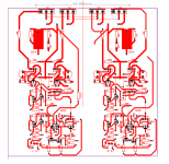
@ostripper here's a PDF ( better quality for zoom ) still working on it.
Glued togheter LTP ? good in practice or I shouldn't bother? . also Vbe multiplier left alone or glue it on pre drivers, drivers, outputs ?. I think pre drivers right? or drivers .
Glued togheter LTP ? good in practice or I shouldn't bother? . also Vbe multiplier left alone or glue it on pre drivers, drivers, outputs ?. I think pre drivers right? or drivers .
Attachments
Not what I meant. I meant this:High level NFB trace is the same phase before or after the inductor... would not matter.
With the modified routing you get a bit more coupling to the ground trace that runs along the bottom of the board. Like I said, it's probably only of academic interest as you're already at the dBGF level with the distortion. That's dB relative to one imperial gnat fart. 🙂
Yes it does. Doug Self wrote about that in his Wireless World article series as well.Another big improvement was to streamline the loop area(s) of the rail feeds.
Having the rails on opposite ends of the PCB (like most kits) sucks....
Tom
Or this if you want to stay away from the decoupling return path:

Just stuff to ponder. That's all.
Tom
Just stuff to ponder. That's all.
Tom
? Vas output is near nfb tho... idk if thats ok@ostripper here's a PDF ( better quality for zoom ) still working on it.
Glued togheter LTP ? good in practice or I shouldn't bother? . also Vbe multiplier left alone or glue it on pre drivers, drivers, outputs ?. I think pre drivers right? or drivers .
#27 post
I wouldn't bother. If you do anything, place the devices close enough to touch in the layout and give them a dab of thermal grease before tying them together with a piece of heat shrink.Glued togheter LTP ? good in practice or I shouldn't bother? .
If it isn't obvious already, I really recommend that you go read Doug Self's articles from Wireless World. You can find Wireless World online here: https://www.worldradiohistory.com/Wireless_World_Magazine.htmalso Vbe multiplier left alone or glue it on pre drivers, drivers, outputs ?. I think pre drivers right? or drivers .
The first article in the 8-part series starts in August of 1993. The eight part is in May of 1994. I think the articles became the foundation of his book, Audio Power Amplifier Design, which is now in its sixth edition. The book obviously features much more content than he was able to fit in the articles.
Bob Cordell also has a good book on power amps. It's a worthwhile read.
Tom
Nice tight loop 👍Input stage NFB is like the example (below-pink trace).... Signal ground reference should be the speaker terminal's main star point G1-speaker.
This is the final solution to get the Wolverine <1ppm/20Khz. Looping the NFB around the rails increased it to 20ppm+.
If you are just shooting for <.02-.05% "normal" distortion , you can be MUCH sloppier !
Edit ... supply grounds (G2-below) go directly to main filter cap star point.
OS
That is the low Z driver pair (to-220's). IPS/VAS plugs in as a modular board. No VAS on that PCB ?? Vas output is near nfb tho... idk if thats ok
#27 post

- Home
- Amplifiers
- Solid State
- NFB Trace on PCB?