I can't be completely sure, but ... ask me how I know it can happen...
Check carefully between all the wiring to each input for inadvertent shorts. With twisted wires close to each other... and a hot iron... and ham fists... I have perhaps maybe once ... or twice... melted the insulation of two wires in a twisted pair.
Not saying that's your cause, but it's a place to look.

Ok, but are this the reason for why one "side" measures a "short"?
For SE input and balanced PCB you only use one jfet buffer pr. channel? ......or?
For SE input and balanced PCB you only use one jfet buffer pr. channel? ......or?
Both at the output connector and on the boards?Balanced output wiring left/right is correct (the same)
Regarding thin wire for the inputs. It seems I can get some AWG 30 silvered wire wrap wire. Is this too thin for input wires?
I think it was the thinnest that was used for wire wrap. AWG 24 were probably more common.
I think it was the thinnest that was used for wire wrap. AWG 24 were probably more common.
... I'm trying to use 0.1mm Dia for input signal wiring; solid copper silver plated
for everything else, I use 0.22mm Dia solid copper silver plated
Yes. Same resistance measured at XLR/SE outputBoth at the output connector and on the boards?
nothing visible on pics
we can guess all day now, but really can't do anything else
freebee needs to desolder volpot wires from pcb, check it, and check continuity between gnd and CW pad on pcb ......
then, either pot is bad (or wires leading to it), or there is short somewhere on pcb
it can be either solder bridge somewhere or wire whisker
pcb itself is proven muriad times, besides other channel with identical pcb doing just fine
so, eyes/brain/elbow time for freebee
The next batch of invitations is being sent out over the next few hours, and passwords in that batch will work for the next 72 hours.
I received a very nice St. Stephen's Day surprise:

I took out the relay and diode to check, but they seem fine.
Have ordered shielded wire (currently using tinned copper multi-strand wire, so I doubt there is a problem there) and will rewire the whole project once it arrives.
Really hope it's something stupid like the wire and not the Cinemag.
it can't be Cinemag
CW pad, when nothing soldered to it - is connected only to common signal of all input relays
I wrote that already
and now - really there is no other way than to use beep on your DMM and eyes and brain and solder iron
you need to check trace connected to CW pad for short to GND, not "relay and diode"
it must be something visible, veeeeery small possibility that pcb got ooked from pcb factory
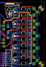
see enclosed, trace marked with yellow line
clean pic too, for clarity
CW pad, when nothing soldered to it - is connected only to common signal of all input relays
I wrote that already
and now - really there is no other way than to use beep on your DMM and eyes and brain and solder iron
you need to check trace connected to CW pad for short to GND, not "relay and diode"
it must be something visible, veeeeery small possibility that pcb got ooked from pcb factory
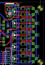
see enclosed, trace marked with yellow line
clean pic too, for clarity
Attachments
Btw, would it be advisable to stack the boards (once everything is working ok)? That way the length of the wires left/right can be kept the same and the PCBs are farther away from the power transformers.
Thanks for your patience with me ZM. 😁 Get beep with DMM in diode setting, when probes between CW+ and K1 (0.2ohm)it can't be Cinemag
CW pad, when nothing soldered to it - is connected only to common signal of all input relays
I wrote that already
and now - really there is no other way than to use beep on your DMM and eyes and brain and solder iron
you need to check trace connected to CW pad for short to GND, not "relay and diode"
it must be something visible, veeeeery small possibility that pcb got ooked from pcb factory
see enclosed, trace marked with yellow line
clean pic too, for clarity
Last edited:
Btw, would it be advisable to stack the boards (once everything is working ok)? That way the length of the wires left/right can be kept the same and the PCBs are farther away from the power transformers.
if that is adequate for your case, why not
Get beep with DMM in diode setting, when probes between CW+ and K1 (0.2ohm)
it's not just K1 pin, trace is common for all 5 relays
if you can't see any whisker or solder bridge (use strong light, lens), then you must desolder all 5 relays
be patient doing that, to not melt them with excessive heat

- Home
- Amplifiers
- Pass Labs
- Iron Pre Essentials Kits For The DIYA Store - Register Your Interest