Good choice Dibya, no point using over larger transformers......
Good luck with your build. Are you building your own pcbs, or buying them from X?
Hugh
Good luck with your build. Are you building your own pcbs, or buying them from X?
Hugh
Hi X, AKSA, other builders,
I was racking my brain looking at the stuffing guide and the AN schematic, and pics of the transistor bolted to the heat sink. I think I finally figured out that I was not looking at the KSC3503, but probably a SA992 or other. The pics showed the small taper of the transistor against the heatsink, which was backwards to how I think the KSC3503 should be mounted.
From the stuffing guide attached and the schematic attached, I believe that I am correct in my reading that the emitter of the KSC3503 is the little dot under the V115 label, which corresponds to the emitter on the schematic which travels through the SA992 and ends up at R115.
Thanks for the help,
Myles,
Using the most current schematic is important for this build, without it, things can get confusing. V113 here is the KSC3503. V115 is the functional equivalent (TTC004B) so you can use that if KSC3503’s are unavailable. V112 is a KSA992.

The KSC3503 is an NPN transistor. The KSA 992 is a PNP transistor.
In schematic convention, the pointy part of the arrow on an NPN transistor is the emitter. For a PNP transistor, the other side of the arrow is the emitter (and the pointy part faces the base). As such the other pin on a PNP transistor is the collector. If you are at all confused while building, always use a transistor tester to verify.

Now, getting back to the Alpha Nirvana:
The emitter of the KSC3503 (V113) connects to the collector of the KSA 992 (V112) and also to one end of R115 resistor. Once you know that then you can just user your multimeter and verify.
Yes the back of the KSC3503 faces the heatsink. But you already knew that AND if you have a KSC3503 in front of you, you can immediately verify with a transistor tester and therefore verify which is front and which is back (See attachments below).
If you do it this way, then you don’t need a ‘stuffing guide’ because you are literally verifying things against the schematic. Stuffing guides are fine, but like all things human they are also subject to errors.
https://www.onsemi.com/pdf/datasheet/ksc3503-d.pdf
https://www.onsemi.com/pdf/datasheet/ksa992-d.pdf
Best,
Anand.
Using the most current schematic is important for this build, without it, things can get confusing. V113 here is the KSC3503. V115 is the functional equivalent (TTC004B) so you can use that if KSC3503’s are unavailable. V112 is a KSA992.
The KSC3503 is an NPN transistor. The KSA 992 is a PNP transistor.
In schematic convention, the pointy part of the arrow on an NPN transistor is the emitter. For a PNP transistor, the other side of the arrow is the emitter (and the pointy part faces the base). As such the other pin on a PNP transistor is the collector. If you are at all confused while building, always use a transistor tester to verify.
Now, getting back to the Alpha Nirvana:
The emitter of the KSC3503 (V113) connects to the collector of the KSA 992 (V112) and also to one end of R115 resistor. Once you know that then you can just user your multimeter and verify.
Yes the back of the KSC3503 faces the heatsink. But you already knew that AND if you have a KSC3503 in front of you, you can immediately verify with a transistor tester and therefore verify which is front and which is back (See attachments below).
If you do it this way, then you don’t need a ‘stuffing guide’ because you are literally verifying things against the schematic. Stuffing guides are fine, but like all things human they are also subject to errors.
https://www.onsemi.com/pdf/datasheet/ksc3503-d.pdf
https://www.onsemi.com/pdf/datasheet/ksa992-d.pdf
Best,
Anand.
Last edited:
Anand,
Thank you for the short course. I know I should trust the schematics, pin outs, results from tester, etc. I just got thrown for a loop from one of the pic's shown of X's build. Will carry on.
Cheers
Thank you for the short course. I know I should trust the schematics, pin outs, results from tester, etc. I just got thrown for a loop from one of the pic's shown of X's build. Will carry on.
Cheers
Thanks Anand, very clear and comprehensive.
Myles, we are ready and happy with your questions!
Hugh
Myles, we are ready and happy with your questions!
Hugh
OK gentlemen, here is a question that has been nagging me:
I have 2 kinds of BD140's for V131, one is a plastic body and one is metal backed. The fully plastic ones have an hfe in the 190 range and the metal backed ones have an hfe in the 150 - 160 range. Which to use, or can I even use a metal backed one without a heatsink ?
This is my last component to solder on the pcb, so I do not want to make an error.
Thanks,
Myles,
You can use either one.
But I would save the metal backed one for another project. And just for your info, if the project requires a heatsink and you are using the metal backed version, you should use an interface material that is thermally conductive and electrically insulating (i.e. non conductive) as the metal backed types of these devices are frequently connected to the collector pin. See respective data sheets. You don’t want that collector pin to be accidentally connected to ground, etc…which means I personally don’t use just grease. I would have to verify first that the heatsink I am attaching isn’t touching ground or wouldn’t accidentally touch ground. That’s too much work. It’s easier to use something like Keratherm, Berquist, etc…and insulate the mounting screw as well with a plastic collar.
Yes, you can use metal backed BD140’s without a heatsink as long as the the power dissipation of that device within the circuit does not exceed or approach it. I first calculate the power dissipation. Then I calculate the theoretical junctional temperature and try to keep it at 125 degrees C or below (within in an enclosed environment i.e. amplifier case). If it is close to 125 degrees C, I determine the size of the heatsink and then calculate the losses that occur due to the interfaces from the transistor to the heatsink to determine what the junctional temperature at the transistor case will be.
FWIW, in this circuit you do not need a heatsink for V131. V131 is a PNP device acting as a CCS controller.
Hfe in this context shouldn’t be relevant as it is usually common to emitter DC gain (ratio of base curent divided by collector current). It is far more relevant to use closely matched Hfe values for example in the input differential pair of transistors in this circuit (the KSA992’s).
Just orient the chosen transistor for V131 properly onto the pcb by associating the emitter, collector and base pins as it pertains to the schematic and solder away!
Best,
Anand.
P.S. If you like, please post several sharp photos (at various views) of your finished Alpha Nirvana board so the collective denizens of DIYAUDIO can look and see if there are any mishaps we can avoid so your maiden voyage is a success!
Last edited:
Again, thank you Anand for your detailed information. I will certainly post a few oic's of the boards once I have them complete. I am just waiting on a few parts to complete. Then I will move on to building up the SLB's and the CPU heatsinks.
May I use that power supply boards fro diyaudio store instead of SLB in dual mono configuration?Yes, more than enough, for monoblock I would recommend a 225VA quality toroid, no more.
Hugh
Attachments
Sure. The SLB provides about 1mV ripple under load. The ripple on a standard CRC is closer to 100mV. It will work but the background noise with SLB will be more quiet.
metanastis,
What is the voltage of your transformers? Please note that with SLB you will require a transformer with higher AC voltage, as there will be a voltage drop of 3 volts.
What is the voltage of your transformers? Please note that with SLB you will require a transformer with higher AC voltage, as there will be a voltage drop of 3 volts.
I have used that pcbs in 2 class A amp projects and my Fluke indicates 0.02mV at 28VDC. I have used the same pcbs with a stabilization circuit using 2N6284 & 2N6287 for positive and negative rail( see image)Sure. The SLB provides about 1mV ripple under load. The ripple on a standard CRC is closer to 100mV. It will work but the background noise with SLB will be more quiet.
 with the same result. I always build a dual mono configuration with 1 trafo per channel.
That’s a nice regulator. I would use it with the Alpha Nirvana if you can. A quiet background is always something I strive for in an audio amplifier.
Hi Morten,
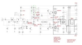
The diodes and zener are correctly installed on the schematic.
They fire ONLY when the voltage at the gate of the upper mosfet exceeds the positive rail, that is (4.7V + 1.6V + 0.65) = 5.95V above the rail.
At this point, the amplifier is clipping since the source of the nmos is almost at the rail itself, the nmos is in saturation (Vds is minimized) and the red led fires demonstrating this event. This flash of red light lasts only an instant, but the eye has latency and will hold this image for 1/24 second. If the waveform is higher than 24Hz, the red led will give an impression of steady state intensity.
You can eschew this diode/zener array if you wish since it only lights up if the amp is clipping on the positive half cycle.
It is a nicety on the design, nothing more.
Hugh

I have used it since 1990 in the 4 of my 4 class A( Elektor AXL class A - Lang 20W class A) amps using the old 2SK135/2SJ50 but it adds extra heat to the sinks and although I use extra large heat sinks, the amp runs really hot for a 1 or 2A QCurrent. It's a superd old fashioned power supply running with the diyaudio/firstwatt CRC board of 60 to 80 mF and there is omV ripple in all my constructions. If you want I can send you the gerber files.That’s a nice regulator. I would use it with the Alpha Nirvana if you can. A quiet background is always something I strive for in an audio amplifier.
Thanks, I didn't realize this. Guess I should have looked for the answer more closely in the thread!Hi Morten,
The diodes and zener are correctly installed on the schematic.
They fire ONLY when the voltage at the gate of the upper mosfet exceeds the positive rail, that is (4.7V + 1.6V + 0.65) = 5.95V above the rail.
At this point, the amplifier is clipping since the source of the nmos is almost at the rail itself, the nmos is in saturation (Vds is minimized) and the red led fires demonstrating this event. This flash of red light lasts only an instant, but the eye has latency and will hold this image for 1/24 second. If the waveform is higher than 24Hz, the red led will give an impression of steady state intensity.
You can eschew this diode/zener array if you wish since it only lights up if the amp is clipping on the positive half cycle.
It is a nicety on the design, nothing more.
Hugh
BTW, has anyone made a comparison between this amp and Lang 20W and say, Hiraga 20W?
It would be great if you could make them available on this forum together with the circuit diagram, probably best in a separate thread.If you want I can send you the gerber files.
I noticed a discrepancy in the 4ohm BOM, the KOA resistors R141 and R142 have the value listed as 0R12 and the part number as BPR58CR22J which is a 0R22 resistor. I apologize if this has already been addressed, but I thought that it may lead to an incorrect value being installed if the individual ordering didn't catch it.
- Home
- Amplifiers
- Solid State
- Alpha Nirvana 39w 8ohm Class A Amp