I see, thank you all!
Here's what I got for now:
1. Decouple the power rails
2. I will make the Power terminal (J2) closer to the output.
3. Use potentiometers to replace a couple of resistors in the Vbe Multiplier and the degeneracy resistors of the IPS
4. Readjust the positions of the output power transistors a bit.
I'll try those
C1 at 2u and R1 at 27k. Set at at about 3Hz highpass cutoff
also add a LPF

Is there a version of the schematic with component values? As a 3 stage LTP design, DC offset should not be an issue. If we see the values, we can help diagnose why you are having offset issues.
On post #9, the caps on the negative rail are backwards. The + should go to ground.
These power supply decoupling capacitors should have their grounds joined together at the same spot that the PSU ground connects. This should also be where the signal ground connects. Search for star grounding for more info. If you use a single ground plane, it's harder to control ground currents and keeping the dirty PSU currents away from the signal ground.
For the VBE multiplier, mounting the VBE transistor directly to one of the drivers will give a better thermal response that mounting to the same heatsink.
I don't see how the heatsinking on the output devices will work (Even with the lowish 15W output). But maybe I just don't understand how you plan to approach it.
This doesn't make sense. R23 is the part of the inductor network. R6 and C22 is your Zobel network. Typically the resistor (R6) is positioned before the cap (C22). I've never seen it reversed like this.
If this is your second PCB design, you may have problems stabilizing the CFP output stage. They are known to be more sensitive to PCB layout. I'd suggest making a provision for degeneration resistors on the driver emitters. You can use links initially and swap out for 10R or 20R if you encounter stability problems. I'd also suggest adding a provision for a ceramic cap from the base to collector of the negative driver Q12. This can also help with stability. It's usually 100p. The same cap is not needed on the positive driver.
As other have suggested a RC low pass input filter would help. Typically 1K for the R as close to the base of Q1 as possible. The value of the C will be based on the dominate pole frequency you designed for. The input low pass filter is typically a bit higher than the dominate pole.
On post #9, the caps on the negative rail are backwards. The + should go to ground.
These power supply decoupling capacitors should have their grounds joined together at the same spot that the PSU ground connects. This should also be where the signal ground connects. Search for star grounding for more info. If you use a single ground plane, it's harder to control ground currents and keeping the dirty PSU currents away from the signal ground.
For the VBE multiplier, mounting the VBE transistor directly to one of the drivers will give a better thermal response that mounting to the same heatsink.
I don't see how the heatsinking on the output devices will work (Even with the lowish 15W output). But maybe I just don't understand how you plan to approach it.
R23 being in series to where the load would be connected is intentional since I would be directly soldering a self-winded inductor across its terminals. So it is a Zobel network
This doesn't make sense. R23 is the part of the inductor network. R6 and C22 is your Zobel network. Typically the resistor (R6) is positioned before the cap (C22). I've never seen it reversed like this.
If this is your second PCB design, you may have problems stabilizing the CFP output stage. They are known to be more sensitive to PCB layout. I'd suggest making a provision for degeneration resistors on the driver emitters. You can use links initially and swap out for 10R or 20R if you encounter stability problems. I'd also suggest adding a provision for a ceramic cap from the base to collector of the negative driver Q12. This can also help with stability. It's usually 100p. The same cap is not needed on the positive driver.
As other have suggested a RC low pass input filter would help. Typically 1K for the R as close to the base of Q1 as possible. The value of the C will be based on the dominate pole frequency you designed for. The input low pass filter is typically a bit higher than the dominate pole.
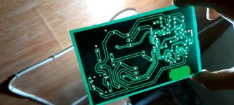
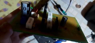
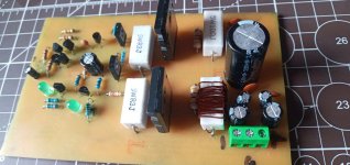
thanks a lot of this one, unfortunately I already etched and built the thing. However no testing or even power up done yet so far. It is the one in the picture attached. At this point, I'm not confident it would function properly. The perfboard just holds the power supply circuit (just a full bridge rectifier plus caps). Attached also is the PCB layout used for the board in the picOn post #9, the caps on the negative rail are backwards. The + should go to ground.
Attachments
Last edited:
This is the one with values including the LTSpice file. I decided to not add an LPF at Q1's input, not a good idea probablyIs there a version of the schematic with component values? As a 3 stage LTP design, DC offset should not be an issue. If we see the values, we can help diagnose why you are having offset issues.
Attachments
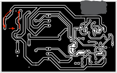
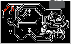
Also, on the PCB layout, I followed the advice to keep the power supply terminal near the output so that there will be short path of the expected large output current back to supply ground. Red is the supply terminal (mid is ground). Green is the output terminal towards load

I ran you asc files - your simulation looks good with respect to DC with the output cap removed. It shows under 20 mV.
You have your lower driver entered wrong. You put the device name in the designator field. So it's behaving as a generic transistor. Also, you should be able to use Cordells MJL3281C/MJL1302C models in place of the 2SC5200/2SA1943 sub-circuits.
Also, ensure you have have the output stage bias set to get realistic results. With a CFP, this is usually somewhere between 20 to 75 mA per device.
I did note that with a 20kHz square wave, a hint of oscillation shows up. Adding 10R of degeneration to the driver emitters cures this. This may not happen in the actual build, but it's worth noting.
Loop gain analysis suggests that you might be able to use a lower value for your miller cap. Potentially around 22p. You'd have to build it and try it. But 47p definitely looks safe and sets your dominate pole around 400 kHz. With 22p, its out around 800 kHz with 14 db and 75 degrees of margin.
R15 & R16 might be a bit low at 47R. If I remember correctly, if these are too low, the output devices can have trouble turning off. If you encounter problems, trying increasing them to 100R.
I'd also recommend again that you make a provision for an input LPF. It's designed to shield the input from high frequency interference. Without it, you could end up picking up radio stations or local interference from things like lighting ballasts.
This is what I got for now, After I am done with the build and testing I'll just come back and see what can I do depending on the outcome. I hope it'll work though 🙂
Decoupling capacitors have kind of a long path between their ground connections. Idea is to minimize the distance for current travel from positive rail to a capacitor then to ground then to another capacitor and finally to a negative rail.
See attached imgs.
You don't need three capacitors. You can use one small ceramic type and another big one electrolytic. For a ceramic 1uF 50V X7R works great and for the big electrolytic one 470uF or 1000uF is nice. You want to place small ceramic capacitors as close to the device that draws current as possible. I'm assuming those devices in your case are output capacitors.
Input high pass filter capacitor can be swapped to a film type. And anywhere where the signal goes it is better to use either film type or C0G or NP0 ceramic type for reduced distortions.
Attachments
Last edited:
You can use electrolytic for input, but you need to make sure you oversize it to push cut frequency way out range of 20Hz to 20kHz. In your case input resistor can be 10K combined with 10uF cap (or bigger is better). If you want higher input resistance, 47K works well with 2.2uF cap (or bigger is better). Handy website to calculate RC filters - http://sim.okawa-denshi.jp/en/CRtool.php
*transistorsYou want to place small ceramic capacitors as close to the device that draws current as possible. I'm assuming those devices in your case are output capacitors.
Er, why?Also - your zobel network is backwards. R23 should come before C7.
Same, it is actually a mistake on my side. If you are to look at my feedback circuit, the resistor always is above then the cap below. I did not make it consistentI've always seen it as R then C to ground
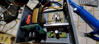
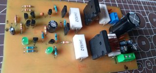
Update on the project. Unfortunately, when I built and tested it. I was getting high amounts of +DC voltage at the output (on the terminals 1,2 of J3). Value is close to the supply rail voltage.

I also made a new simplified version. I stripped a some of components. Like for example, instead of a two transistor current source, I made a diode + resistor bias for the current source. I also removed Q7 and R12 which was a very bad I idea. It could have saved me frying Q11 and Q9 as well as R33 when I was testing it.
Also, I removed the Vbe multiplier and went for a a simple two-diode bias for the CFP stage, I came with a diode + resistor instead of two diodes.
This is only for testing though, I am planning to get to the original and get each stage working. I did not bother adding heatsinks to the large transistors yet as I was only troubleshooting on low power.
Attachments
- Home
- Design & Build
- Construction Tips
- Need opinions on my PCB 3-stage amp design. Will it work?