However, result is still the same, the problem indeed lies around the input as well as VAS stage. But I was able to find something abnormal. I bought new parts and replaced the burnt ones from the previous testing.
I was able to measure about 27V across R8 when it should only be around 1V.

I was able to measure about 27V across R8 when it should only be around 1V.
I look closely, it seems looks like all the transistors are reversed.
Did you make the board with the solder side and the component side of the photosensitive film reversed?
Did you make the board with the solder side and the component side of the photosensitive film reversed?
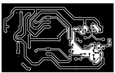
I had to print the layout in reverse so that the ink side would be touching the copper side, It is a single sided PCB.Did you make the board with the solder side and the component side of the photosensitive film reversed?
For the small signal transistors, there should be no issue with reversing of pins since I am using this kind of footprint for the small signal transistors. It's obvious where they should face. But there still is a possibility of my error that I had them upside down. I've attached the KiCAD file as well as the layout when I would etch (mirrored).
Attachments
Last edited:
I am not using KICAD. Even if a KICAD file is attached, it cannot be viewed.
I don't understand the pattern diagram either. Make a diagram like brian92fs showed in #25. Also, please clarify whether it is a component side view or a solder side view.
Check yourself well before that.
I don't understand the pattern diagram either. Make a diagram like brian92fs showed in #25. Also, please clarify whether it is a component side view or a solder side view.
Check yourself well before that.
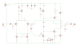
It is component side view. Be warned, it uses different component numbering. I've attached it with the schematic that has the same numbering. I have removed the ground plane for now for clarity of view. Those unconnected pins seen in the image are supposed to be ground.
Attachments

all the transistors are reversed.
I think I messed the whole thing up by printing the layout mirroredThe pinouts appear to be reversed
- Home
- Design & Build
- Construction Tips
- Need opinions on my PCB 3-stage amp design. Will it work?