I am really pulling my hair out with this amplifier. I just do not know what direction to go with it. hopefully i can get a little more help or advise on this site ...cause im almost ready to throw in the towel.
If you want to troubleshoot this thing you need to take a bunch of voltage readings until you find something wrong. If the there is a big DC offset at the output then the input stage should be trying to correct for it. Is it? If it is, then follow to the the next stage to see if the transistors there are responding to the correction signal from the input stage. At some point the correction signal will get lost or become ineffective. You need to find where that point in the circuit is.
where does the voltage come from all pins of Q9 66vdc high voltage. .the collector goes to the pos rail, i understand, but base? where the high dc volt come from
When a bipolar transistor is working correctly (in the linear region), the Vbe is always about 0.6VDC.
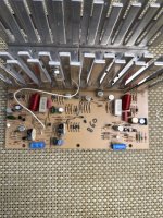
hello rayma, i have removed every semiconductor on the board and tested them with a peak transistor tester and double checked them with the diode function of my dvom. they all tested good. i have also tested all the diodes 1n5004.1n5003,1n4150 ..also tested and replaced all the zener diodes 1n4742a i have tested all my mosfets with the peak transistor tester and with a diode check between the drain and the source..all showing open, then i touch the pos + lead to the gate and then the mosfets showed contuinuity.......after that i discharged the mosfet with my finger and there was no connection from drain to source.
Never directly touch the gate, since the voltage breakdown can be as low as 20V.
Failure may not immediately occur, but can happen later on due to weakening of the gate structure.
Have you tested all the other parts? What about the continuity of the device tabs to the sink?
Have you fixed that? Are there isolation pads?
Failure may not immediately occur, but can happen later on due to weakening of the gate structure.
Have you tested all the other parts? What about the continuity of the device tabs to the sink?
Have you fixed that? Are there isolation pads?
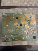
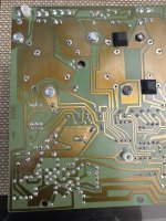
If everything you tell us is the same, then go inspect your PCB again, there is a copper whisker shorting something to something else. Or a dry solder joint or hairline crack.When a bipolar transistor is working correctly (in the linear region), the Vbe is always about 0.6VDC.

Start with both working and non-working PCB, turn them copper side up and measure between each solder point and compare voltages. Start at the input and work your way to the output. Remove the FB resistors on both so that you don't find the output on the inverting amp input, they should both be held a zero volt. It may be better to pull both inverting and non-inverting input through a resistor to ground, so they are physically at zero volt.
Last edited:
This amp is super simple, but there are some odd things I would not have done. I think that one of the driver transistors is stuffed or in the wrong position/orientation.
hello rayma, i have removed every semiconductor on the board and tested them with a peak transistor tester and double checked them with the diode function of my dvom. they all tested good. i have also tested all the diodes 1n5004.1n5003,1n4150 ..also tested and replaced all the zener diodes 1n4742a i have tested all my mosfets with the peak transistor tester and with a diode check between the drain and the source..all showing open, then i touch the pos + lead to the gate and then the mosfets showed contuinuity.......after that i discharged the mosfet with my finger and there was no connection from drain to source.
Never directly touch the gate, since the voltage breakdown can be as low as 20V.
Failure may not immediately occur, but can happen later on due to weakening of the gate structure.
Have you tested all the other parts? What about the continuity of the device tabs to the sink?
Have you fixed that? Are there isolation pads?
The amplifier never came with insulators . The mosfet had thermal paste and directly mounted to the heatsinlks. What do you mean by device tabs to the heatsinks? I don't understand.Never directly touch the gate, since the voltage breakdown can be as low as 20V.
Failure may not immediately occur, but can happen later on due to weakening of the gate structure.
Have you tested all the other parts? What about the continuity of the device tabs to the sink?
Have you fixed that? Are there isolation pads?
Hello Sir. I have removed all the mosfets and would like to continue testing. To find the problem on the board . What would you recommend?This amp is super simple, but there are some odd things I would not have done. I think that one of the driver transistors is stuffed or in the wrong position/orientation.
The amplifier never came with insulators . The mosfet had thermal paste and directly mounted to the heatsinlks. What do you mean by device tabs to the heatsinks? I don't understand.
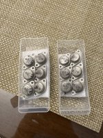
Post photos of the removed output devices, on both sides.
It appears they have TO3 cases, which need isolation with (usually) mica insulators.
Their metal case IS the collector/drain terminal.
Last edited:
The mosfet test was something I learned on YouTube. What would you recommend now that the mosfets have been removed. I am sure the problem is on the board and nothing else.Never directly touch the gate, since the voltage breakdown can be as low as 20V.
Failure may not immediately occur, but can happen later on due to weakening of the gate structure.
Have you tested all the other parts? What about the continuity of the device tabs to the sink?
Have you fixed that? Are there isolation pads?
Post photos of the removed output devices, on both sides.
It appears they are TO3 which need isolation with usually mica insulators.
Attachments
Post photos of the removed output devices, on both sides.
It appears they are TO3 which need isolation with usually mica insulators.
Attachments
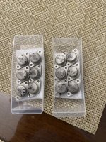
Those sure look like TO3. They should have insulators if there is exposed metal on the bottom, which we would presume there is.
Over the years I have had about six of these shoe box amplifiers. None of them came with to3 insulators
Hello Sir. I have removed all the mosfets and would like to continue testing. To find the problem on the board . What would you recommend?
Attachments
- Home
- Amplifiers
- Solid State
- can anyone offer help understanding the flow of this circuit