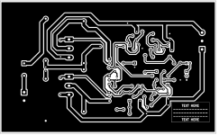
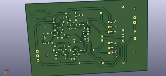
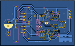
I need some reviewing if my PCB design for this 3-stage 15W amplifier would work with my component placement. This is the 2nd PCB I have designed and would etch it myself. I am designing it in KiCAD

Attachments
Last edited:
I got gaps behind the large transistors since I would be attaching heatsinks there. The three medium sized transistors are the driver and the VBE multiplier in the middle. The large ones are the output ones, I do not know if it is ok positioning those two resistors behind each of them.
R23 being in series to where the load would be connected is intentional since I would be directly soldering a self-winded inductor across its terminals. So it is a Zobel network

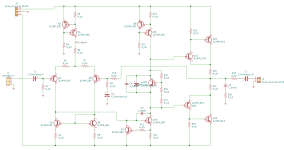
I only have C1 and R1 as the input filter. I have C1 at 2u and R1 at 27k. Set at at about 3Hz highpass cutoff. As for the rail coupling, would 100u-10u-100n work?
CTRIX is talking about rail decoupling as an example 100uF +100nF from each rail to ground. Lack of decoupling would result in what is called motor boating.
I also did not see, I have to reload to see new comments. But just to be sure, like these right?Sorry I was probably writing the same time your did.
I am sorry, I did not understand the terms. wdym by "potentials will race on the ground as they wish". Also, about the input filter I am thinking the R1 and C1 highpass filter at Q1's base is not adequate?Not good PCB, potentials will race on the ground as they wish. Non-RC filter on input will give hard oscillations. Try not to use polygonal type of ground if you can't imagine/know the current's map.
sorry. 🙄
I don't see place for heatsinks. And outputs transistors are too close to each other... 🙄
That I am 50/50 on implementing it. I did print the black and white version and I think I can. I would be using a presensitized PCB and transfer the pattern via UV light exposure. I've been hearing and watching videos it can do thin traces.The trace gap is quite narrow, will you be able to implement that successfully?
The output cap C7 I need it for a different reason. When I do not have it the quiescent current on my output stage would be imbalanced for a bit. For example, the current through R20 is 70mA but there is 65-68mA through R21. But when I added C7, they become almost equal.You do not need the output cap unless you are afraid of DC when something goes wrong in the amp.
Maybe place the power connector next to the output connector so that the ground current to the speaker is short.
I trust that you are not going to test the amp from first switch on with an expensive speaker, normally one would use a load resistor.
The DC offset can be corrected by R4 and R7, it may be more practical to use a PCB mounted potentiometer here to adjust for 0V DC offset.
Replacing R16 and R17 with a PCB potentiometer would allow you to adjust bias current practically. I just need to warn you that in a simulation all the components are perfect and in practice not. Being able to make adjustments on the fly is a smart thing to do.
For the sake of a last comment, I would place decoupling diodes between the power devices and the front end and feed power near the power devices. This is because you do not want the power supply to be modulated by the music current.
- Home
- Design & Build
- Construction Tips
- Need opinions on my PCB 3-stage amp design. Will it work?