All good stuff guys. Amazing work George.
I got mine rigged up over the last couple days. Initially thought I had an issue as I had 0v at TP10....yes 10. Soon realised my mistake...that isn't TP9 next to TP8!
Then got it into system last night and no music....hhmm. Oh.....I forgot to populate the electrolytics .
I'm dangerous sometimes!
Richard I (again dangerously) assume that 18.3v is safe? My shunt settles to 18v with thermal equilibrium but starts off at 18.3 or so
Jim - sure 18.3V is perfectly OK. Without 'lytics you'll have no signal at the output pins, but you probably already figured that!
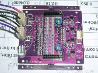
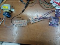
Soldering at main board per Phase 1 of Soldering Guide accomplished.
Below are the DC measurements (Phase 1)
PSU:
+18.05V 68mA draw
-18.07V 16mA draw
T.P. Vdc (rel.TP 0)
1 7.14
2 7.14
3 0.624
4 -2.52
5 15.2
6 7.16
7 7.16
8 8.33
9 8.33
C1+ 18.04
C2- -18.07
C6+ 7.78
C6- -18.07
C7+ 18.04
C8+ 8.33
C9+ 8.33
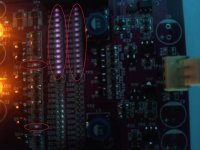
All IR LEDS operate (visible through mobile phone's camera).
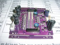
Then soldered electrl. caps.
And my beloved companion in day to day home-work
George
Below are the DC measurements (Phase 1)
PSU:
+18.05V 68mA draw
-18.07V 16mA draw
T.P. Vdc (rel.TP 0)
1 7.14
2 7.14
3 0.624
4 -2.52
5 15.2
6 7.16
7 7.16
8 8.33
9 8.33
C1+ 18.04
C2- -18.07
C6+ 7.78
C6- -18.07
C7+ 18.04
C8+ 8.33
C9+ 8.33
All IR LEDS operate (visible through mobile phone's camera).
Then soldered electrl. caps.
And my beloved companion in day to day home-work
George
Attachments

Last edited:

What is the search term for the connectors you use Richard.? Tried Molex KK and Minifit and JST but they aren't these are they! I have a box of them from Ali but it doesn't really give a repeatable reference to what they're called!
Had to ask wifey for the magic passphrase which is 'KF2510' as in here : https://www.aliexpress.com/item/328...!sea!HK!2609685283&curPageLogUid=dTUJlqIogb88
Keep having a go at listening ...I have it working but my shunt PSU keeps shutting down on the neg rail. Fortunately losing a rail doesn't cause any I'll effects to the speakers.
Fine sat on the bench but once in the rack playing music it plays up. Maybe overheating as the sinks of the shunt are hard to up under a rack shelf but they done feel hot.
But hey....the time I get with it sounds mighty impressive!
Fine sat on the bench but once in the rack playing music it plays up. Maybe overheating as the sinks of the shunt are hard to up under a rack shelf but they done feel hot.
But hey....the time I get with it sounds mighty impressive!
Well what a torid afternoon. I managed to blow up my dark IV and a PSU. Silly reverse polarity **** up. Was trying a cap mx PSU and they don't like that so think that's blown some actives.
Blew a rail cap on the IV. Removed and repowered . 2 X yellow LEDs...... hopeful at this point but checked the voltages over the board.
TP1 -3.9
TP1 -3.8
TP3 - 3.1
TP4 -3.1
TP5 +15.3
TP6 +14.6
TP7 +14.6
TP8 +15.8
TP9 +15.8.
Which transistors have I blown ..all of em?!
This project seems fated!
Edit....Q1 and Q2...are they the same as 3 thru 7? They look darker/ less shiny .
Sorry to burden with fault finding
Oh dear!
Were those TP measurements taken with the shorting links (or filter) in position? The fact that the later ones are all very high makes me think 'no'. Debug is practically impossible without a filter or link DC path.
Q1 and Q2 are different - they're MOSFETs, the rest of the Qs are bipolar.
Were those TP measurements taken with the shorting links (or filter) in position? The fact that the later ones are all very high makes me think 'no'. Debug is practically impossible without a filter or link DC path.
Q1 and Q2 are different - they're MOSFETs, the rest of the Qs are bipolar.
There's hope yet then as no I didn't have the jumpers in...will report back. Keep everything crossed!
And the capmx PsU I was trying comes up pretty slowly so hopefully I pulled the power soon enough. Time will tell! Cheers Richard.
It's fine....all TPs measure up ....thank god for that!
🙂 you do indeed remember correctly.There's more hope for discrete circuits than with opamps on polarity reversal. I recall @Grarea sent his Kubelik to kingdom come with a similar trick but it turned out only the opamps blew up, all the rest survived. If I remember correctly.
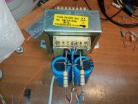
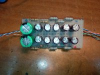
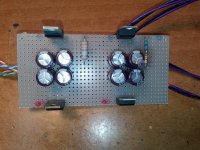
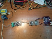
I made some progress the last two days.
This project is friendly to PSU variants.🙂
I started from the basics with basic module units in mind. A transformer/rectifier with the bulk capacitors as the -electrical- noisy set. Then RCRC filter modules for the +/-18Vdc Dark Led and the +/5Vdc Mini Ref. DAC. Then the voltage stabilizers modules. For now they are the bare basic LM7818/LM7918 and LM7805/LM7905. A few more voltage stabilizer units of different design will be build for to compare and measure.
Both the Dark Led and the Mini Ref. DAC are heavier in current demand at their plus compared to their negative psu rail. A load balancing resistor downstream of the supply chain is required for bringing the amperage in equilibrium. The Dark Led requires a 340 Ohm btn minus and ground for +/-62mA draw. The light DAC requires 860 Ohm btn minus and ground for +/-12mA draw.
George
Attachments
-
 1 Tr-rect w bulk CR module.jpg439.4 KB · Views: 119
 -
 2 crcr module.jpg494.9 KB · Views: 111
 -
 3 V-stab module w78xx-79xx.jpg482.5 KB · Views: 107
 -
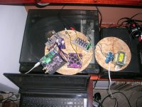
 4 upper side assy.jpg568.9 KB · Views: 116
 -
 5 under side assy.jpg508.6 KB · Views: 155
 -
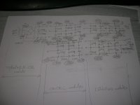 6 final schem with78xx-79xx.JPG504 KB · Views: 157
 -
 7 testing load resistors.jpg499.6 KB · Views: 157
The USB to I2S is on lease from the nearby opamp-less Abbado.
At first I had no sound. It was the filter board missing.
After correcting this minor mistake , the setup in rudimental stage is doing it’s job for some hours now.
The deep and authoritative bass caught my attention from the first notes.
Clear and open sound, no noises.
Thelonious Monk, Art Blakey and Dave Brubeck asked me to pass on their compliments to Abrax and Wife for Dark Led is treating their music well.


George
At first I had no sound. It was the filter board missing.
After correcting this minor mistake
, the setup in rudimental stage is doing it’s job for some hours now.The deep and authoritative bass caught my attention from the first notes.
Clear and open sound, no noises.
Thelonious Monk, Art Blakey and Dave Brubeck asked me to pass on their compliments to Abrax and Wife for Dark Led is treating their music well.
George
Attachments
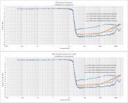
I will try to give some data on FR of my filters.I shall be interested to see how that choice impacts the frequency response of the final filter.
I had done some measurements of the stand-alone filter board terminated to it's designated load of 1500Ohm.
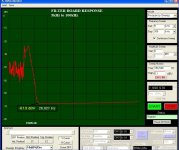
Initially providing signal from my soundcard (Ro:150Ohm) and using REW doing a freq sweep up to 96kHz, I captured the filter output with the soundcard (Rin:1Mohm) using oscilloscope (x1) probes. Results (Vin-Vout) were expectable and good within the passband but with poor results at the cutoff region. See 1st attachment.
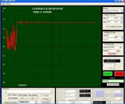
Then I made use of an ancient (DOS environment) analyser, just to see the frequency band btn 20kHz and 100kHz (Ro:50Ohm, Rin:1MOhm, x1 probes). Rejection band behavior much better but still a shallow cut-off. See 2nd and 3rd attachment.
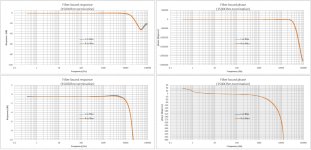
Then I turned to manual point to point measurement using a DDS signal generator (Ro: 50Ohm) and a DS oscilloscope (Rin:1MOhm) x1 probes. 5Hz to 20MHz. Various attempts with improving results. See 4th attachment.
The best achieved results can be seen in 5th attachment. -80dB from 35kHz to 3.7MHz and then slowly rising (test fixture details matter!)
George
Attachments
Last edited:
George, lots of eye candy there, thanks. There is one thing I feel its important to point out - this filter is designed to be driven by a current source, not a voltage source. Current sources have very high output impedance, I will check in LTSpice if I get similar results to you when driven by 150ohm. I began the design of the filter with the online facility at https://rf-tools.com/lc-filter/ and set its input impedance to 150kohm (100X the termination resistance).
As signal generators generally only work in voltage mode, to verify the filter in isolation I drive the siggen output through a 75kohm resistor as 50X the termination resistance makes little difference from infinity in terms of the FR. Of course this gives significant attenuation at the output but the signal level is normally high enough to see clearly above the noise with the max output (20V p-p) of my generator.
As signal generators generally only work in voltage mode, to verify the filter in isolation I drive the siggen output through a 75kohm resistor as 50X the termination resistance makes little difference from infinity in terms of the FR. Of course this gives significant attenuation at the output but the signal level is normally high enough to see clearly above the noise with the max output (20V p-p) of my generator.
Hi Abrax, thank you very much for responding on this.
I was aware of the effect of the source impedance on the results but in praxis I couldn't do any different: In my setup, I already had to read sub milivolt levels at the cut off region. Adding a high level resistor in series with the signal source made readings there impossible.
Regarding LTSpice sims shows a big difference, more than 20dB in the cut off region and some difference at the transition band.
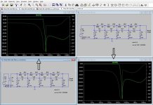
But the whole validity of the sim is in including the component's parasitics as well as the parasitics due to component placement. See my crude attempts in 1st attachment.
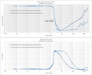
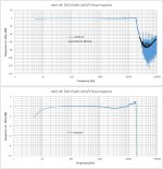
Two days ago, as I built the PSUs, I made a FR of the whole set (mini Ref. DAC +Filter board+Dark LED I/V on one channel using a USB digital signal input and reading the buffered output with the sound card. Results at the 2nd and 3rd attachments.
Don't pay attention for the moment at the low freq droop, for it's open loop measurement and shows the LF response of the sound card's input. I will try to make the proper compensation as soon as I am in position to return to the measurements (I am left with no USB to I2S converter).
George
PS. I forgot to thank you for the link to the online filter simulator.🙂
I was aware of the effect of the source impedance on the results but in praxis I couldn't do any different: In my setup, I already had to read sub milivolt levels at the cut off region. Adding a high level resistor in series with the signal source made readings there impossible.
Regarding LTSpice sims shows a big difference, more than 20dB in the cut off region and some difference at the transition band.
But the whole validity of the sim is in including the component's parasitics as well as the parasitics due to component placement. See my crude attempts in 1st attachment.
Two days ago, as I built the PSUs, I made a FR of the whole set (mini Ref. DAC +Filter board+Dark LED I/V on one channel using a USB digital signal input and reading the buffered output with the sound card. Results at the 2nd and 3rd attachments.
Don't pay attention for the moment at the low freq droop, for it's open loop measurement and shows the LF response of the sound card's input. I will try to make the proper compensation as soon as I am in position to return to the measurements (I am left with no USB to I2S converter).
George
PS. I forgot to thank you for the link to the online filter simulator.🙂
Attachments

Last edited:
- Home
- Vendor's Bazaar
- Dark LED passive filter-I/V stage for NOS DACs