What is the simplest way to make a circuit that will allow AC or DC voltage to pass UP TO a value that you set or specify, with decent millivolt accuracy in terms of the voltage limiting feature?
Considerations
Considerations
- When the limit voltage is reached, the circuit should continue to allow voltage equal to limit value to pass (it must not cut it to zero).
- If necessary to choose between AC or DC, then AC would be preferred.
- The circuit will should have four connection points, two "input" which can be 0-35V (ac or dc; input range can be adjusted to make it work), and two "output" ports
- The output must pass from 0.01 mV up to the voltage limit set.
- If input was AC output must be AC; if input was DC then output should also be DC.
- Ideally, the circuit should be passive and should not require power to operate.
- Should be able to handle at least 100 mAh of current.
So the signal has to be compared with a user setting with millivolt accurecy without active parts.
I'd say a no go.
Passive 'reference levels' can be made with schottky, germanium and/or silicon diodes in a string network with resistors, adjustable with a multipole / multiposition switch, taken into consideration the logarithmic nature of the signals when calculating the many involved resistors (100+?) in the network.
Another approach could be with a FET as a adjustable attenuator, but levels up to 35V and 100mA (dc/ac) are very challenging.
Maybe it has been invented already, but not to my knowledge.
I'm not an electronics design expert but the idea I had in my mind was something like this:
Now I don't think this will work up to 35V and/or 100 mAH but I think it's a starting point. I also foresee that there are some issues here, like making this work with AC and DC. I think this would be fine with DC but not AC. My idea to make it work with AC and DC is to use a buck converter to power the logic portion of the circuit while still allowing the untouched original voltage (whether AC or DC) to flow through a transistor. This logic circuit would then either allow full voltage to pass OR it would pass the full voltage through a voltage divider once it reaches the set limit. Hoping someone who has more experience with circuit design can provide some ideas here.
- Using a zener diode in reverse, connected to an NPN transistor
- The other lead of the transistor will flow all voltage below the value of the zener diode
- When the voltage gets high enough to flow through the diode, the transistor will open the free-flowing circuit and switch to the one with the diode
- Because we will roughly know that the voltage coming from the diode will be a fixed value, we can use a voltage divider to further tune the output voltage
Now I don't think this will work up to 35V and/or 100 mAH but I think it's a starting point. I also foresee that there are some issues here, like making this work with AC and DC. I think this would be fine with DC but not AC. My idea to make it work with AC and DC is to use a buck converter to power the logic portion of the circuit while still allowing the untouched original voltage (whether AC or DC) to flow through a transistor. This logic circuit would then either allow full voltage to pass OR it would pass the full voltage through a voltage divider once it reaches the set limit. Hoping someone who has more experience with circuit design can provide some ideas here.
Current is measured in ampere, not ampere-hour. Just saying...
A BJT will need at least 600-700 mV (and some amount of base current) to conduct. The 600-700 mV is actually a diode drop. You can find this voltage from the Ebers-Moll equation and you'll find that it depends on temperature so unless you submerge your clamp in a temperature controlled bath of some sort you'll never reach mV precision. The BJT is also an active device, so it fails your "preferably passive" requirement.
Zener voltages depend on temperature as well.
Chapter 24 in Douglas Self's "Small Signal Audio Design" book (2nd ed) deals with speciality circuits, including limiters. That could be a good place to start.
What is the application for this circuit?
Tom
A zener in reverse is a normal diode, no zener function possible.
- Using a zener diode in reverse, connected to an NPN transistor
A transistor has three legs. One leg is connected to this zener in reverse, the other is flowing voltage...?
- The other lead of the transistor will flow all voltage below the value of the zener diode
And the third???
Lorem ipsum dolor sit amet... I cannot get the picture here. A free flowing circuit and switching (?) to the one... &c.
- When the voltage gets high enough to flow through the diode, the transistor will open the free-flowing circuit and switch to the one with the diode
A voltage coming from a diode will be fixed, and a voltage divider to tune the output voltage. Ehmm...
- Because we will roughly know that the voltage coming from the diode will be a fixed value, we can use a voltage divider to further tune the output voltage
I'm pretty much sure the idea won't work at all, not small level mV's, up to 35V, ac or dc alike. But your foreseeing issues is ok.Now I don't think this will work up to 35V and/or 100 mAH but I think it's a starting point. I also foresee that there are some issues here, like making this work with AC and DC. I think this would be fine with DC but not AC. My idea to make it work with AC and DC is to use a buck converter to power the logic portion of the circuit while still allowing the untouched original voltage (whether AC or DC) to flow through a transistor. This logic circuit would then either allow full voltage to pass OR it would pass the full voltage through a voltage divider once it reaches the set limit. Hoping someone who has more experience with circuit design can provide some ideas here.
A buck converter... a logic portion of the circuit... passing full or through a divider...
"Ideally, the circuit should be passive and should not require power to operate."
I'm not adding smilies of any kind, because there are non to express my utter bafflement.
This is your challenge: make a sketch (a rough handdrawing is sufficient) of the involved parts and functional blocks and post it here to give us an idea how you imagine how this contraption should work.
The idea of a passive limiter is not strange, but given the nature and possiblities of electronic components, some minor limitations are to take into account when designing such a circuit (-> #2).
Or follow the route of #4 better.

Current is measured in ampere, not ampere-hour. Just saying...
A BJT will need at least 600-700 mV (and some amount of base current) to conduct. The 600-700 mV is actually a diode drop. You can find this voltage from the Ebers-Moll equation and you'll find that it depends on temperature so unless you submerge your clamp in a temperature controlled bath of some sort you'll never reach mV precision. The BJT is also an active device, so it fails your "preferably passive" requirement.
Zener voltages depend on temperature as well.
Chapter 24 in Douglas Self's "Small Signal Audio Design" book (2nd ed) deals with speciality circuits, including limiters. That could be a good place to start.
What is the application for this circuit?
Tom
Yeah, I got that acronym wrong but people can still infer that it means the amount of current that the circuit can handle. There is no specific application, I just liked the idea of making a fairly accurate 'universal' voltage regulator that doesn't require its own separate power source. Unfortunately, it looks like the idea I proposed (due to a lack of suggestions from the experts) would not work without its own power supply.
A zener in reverse is a normal diode, no zener function possible.
A transistor has three legs. One leg is connected to this zener in reverse, the other is flowing voltage...?
And the third???
Lorem ipsum dolor sit amet... I cannot get the picture here. A free flowing circuit and switching (?) to the one... &c.
A voltage coming from a diode will be fixed, and a voltage divider to tune the output voltage. Ehmm...
I'm pretty much sure the idea won't work at all, not small level mV's, up to 35V, ac or dc alike. But your foreseeing issues is ok.
A buck converter... a logic portion of the circuit... passing full or through a divider...
"Ideally, the circuit should be passive and should not require power to operate."
I'm not adding smilies of any kind, because there are non to express my utter bafflement.
This is your challenge: make a sketch (a rough handdrawing is sufficient) of the involved parts and functional blocks and post it here to give us an idea how you imagine how this contraption should work.
The idea of a passive limiter is not strange, but given the nature and possiblities of electronic components, some minor limitations are to take into account when designing such a circuit (-> #2).
Or follow the route of #4 better.
So tell me what a zener diode does when the polarity is reversed (against its normal diode function) and the "zener voltage" of the diode is reached?
Then tell me how the same diode will behave when the voltage is below the zener voltage?
Then transistor is a switch, so the idea is that the input voltage would normally be connected to two of the 3 legs of the transistor, such that there is a kind of Y- junction where one leg has the zener diode and the other does not. When the voltage reaches the zener voltage, the current will flow through the diode into the transistor leg, which then causeallows us to then enforce the desired voltage limit. Get it?
INPUT ---> NPN_COLLECTOR ---> OUT1 ---> GROUND
INPUT ---> ZENER ---> OUT2 ---> NPN_BASE
NPN_EMITTER ---> GROUND
INPUT is the same voltage source, which is connected to the collector as well as the base of the transistor.
The zener diode will stop current from flowing to the base of the transistor as long as the voltage is below the zener voltage, so OUT2 will be "open" and OUT1 will be closed. When the zener voltage is reached and the diode allows current to flow to the base, OUT1 is "open" and OUT2 is "closed".
OUT2 will be the limited voltage while OUT1 is free-flowing voltage.
"Not require power to operate"
Baffles you? So you are unfamiliar with passive circuits that do not require their own power supply? Should you really be responding to this thread if your knowledge of such basic concepts is lacking?
This what I can make of it.INPUT ---> NPN_COLLECTOR ---> OUT1 ---> GROUND
INPUT ---> ZENER ---> OUT2 ---> NPN_BASE
NPN_EMITTER ---> GROUND
You better make a sketch yourself.
Attachments
A modified DI, to have the unbalanced jacks isolated too. Added were the two 1:1 audio transformers. Humless, of course.So you are unfamiliar with passive circuits that do not require their own power supply? Should you really be responding to this thread if your knowledge of such basic concepts is lacking?
(Drawn in excel for the fun of it, picture scaled and b/w inversed to have it glued on the box.)
Attachments
https://en.wikipedia.org/wiki/Zener_diodeSo tell me what a zener diode does when the polarity is reversed (against its normal diode function) and the "zener voltage" of the diode is reached?
Then tell me how the same diode will behave when the voltage is below the zener voltage?
When the anode of a zener diode is at a higher potential than the cathode the zener diode will conduct like any other diode. When the zener diode is reverse biased, i.e., biased with its cathode at a higher potential than the anode, it will undergo zener breakdown (assuming it is a zener diode) or avalanche breakdown (for higher voltage "zener" diodes) once the potential difference (Vk-Va) exceeds the breakdown voltage.So tell me what a zener diode does when the polarity is reversed (against its normal diode function) and the "zener voltage" of the diode is reached?
Then tell me how the same diode will behave when the voltage is below the zener voltage?
Yeah, but that's actually fundamentally broken.Then transistor is a switch, so the idea is that the input voltage would normally be connected to two of the 3 legs of the transistor, such that there is a kind of Y- junction where one leg has the zener diode and the other does not. When the voltage reaches the zener voltage, the current will flow through the diode into the transistor leg, which then causeallows us to then enforce the desired voltage limit. Get it?
Ever heard the expression that a picture is worth a thousand words?INPUT ---> NPN_COLLECTOR ---> OUT1 ---> GROUND
INPUT ---> ZENER ---> OUT2 ---> NPN_BASE
NPN_EMITTER ---> GROUND
It sounds like you're describing a shunt regulator. But then again without a schematic it's hard to tell. You could help yourself considerably by drawing a schematic. That would also help those of us who try to help you such that we can provide better help.
There's nothing in your ASCII netlist that would limit the base current, so the transistor would blow. You'll also short out the incoming power supply through the NPN, thereby blowing the NPN without some sort of current limit, hence my comment above that your circuit is fundamentally broken.
Yeah. That is baffling. Your original post said the circuit should be passive. The circuit you describe above uses active devices (the NPN) so it fails that requirement. It also requires power to function. The current through the zener has to come from somewhere. It seems like you are working from a different definition of "active device" than everybody else and then get upset when we can't read your mind."Not require power to operate"
Baffles you? So you are unfamiliar with passive circuits that do not require their own power supply? Should you really be responding to this thread if your knowledge of such basic concepts is lacking?
I suggest you look at a basic zener regulator. It's not the greatest voltage regulator out there as the output voltage depends pretty heavily on temperature and its output impedance is on the high side. But I think it will do what you want it to and it only consumes the zener current and base current for the emitter follower pass transistor. Here's an example schematic of one:
You could also look at the LM317. Here's the data sheet: https://www.ti.com/lit/ds/symlink/lm317.pdf
Figure 9 shows an adjustable voltage regulator. You can adjust it down to 1.3 V and up to (Vin-3) volt. It does contain active devices, though. And it does consume about 10 mA.
Best of luck.
Tom
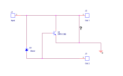
This what I can make of it.
You better make a sketch yourself.
This should work for DC. I know it won't work with AC as it is depicted now, but I think that it can be made to work with AC with some creativity. The point here is whether or not this approach could work, even if it misses some of the originally stated features - the one thing it must do is limit the voltage reliably.
I have intentionally left the drawing open-ended, but if you refer to my previous textual description of the circuit whose image is in this post, you should be able to see what I am trying to do. Starting from the left, you have the voltage input as DC. The voltage source then connects directly to the collector of the NPN and also to the base through a zener diode (it doens't have to be a zener but I can't think of a simple component that would work as intended).
OUT1 (topmost): The zener will cause all of the current to flow through NPN collector to emitter as long as the voltage is below the zener voltage. It is tapped so that one of the outputs is the voltage below the limit, and we want this coming out as "untouched" as possible.
OUT2 (bottom): When the voltage of the source increases to the zener voltage, current will hit the base and cease to flow from the collector. Here I tapped the circuit between the zener and the base of the NPN, because this will be the "limited" voltage. While not shown here, the actual voltage coming from the zener could further be adjusted with a simple voltage divider that taps back into the wire coming out of the emitter of the NPN, with the divided voltage becoming the new OUT2.
@tomchr To address the concerns you raised about this being broken - the voltage source should not exceed the ratings of the components used, such that both the diode and transistor should both be fine without any special protection...and I can't think of any way to protect the transistor other than putting a resistor before it or after...and as you can see from the image, I am trying to leave the original voltage source as undisturbed as possible.
As for the NPN requiring power to function, sure, but does it require EXTERNAL POWER. While we can split hairs about how we interpret the meanings of words, I've made it quite clear that what I mean by passive circuit id one that will do its job without the need for external power.
Now that I drew a diagram, is there any way you would improve my circuit so that it would work if you think that it won't work as-is?
You said in ASCII:The point here is whether or not this approach could work...
INPUT ---> NPN_COLLECTOR ---> OUT1 ---> GROUND
But in your drawing the emitter is connected to out1.
So, output 1 is connected to ground?
Hmm......I've made it quite clear...
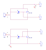
I've tried to redraw your sketch (top) and put it in a more formal way (bottom).
So far as much you have tried to make it quite clear, with all respect, even with all other to imply other and further needed components to obtain your goal, this approach, dc or ac likewise, cannot and will not work as intended.
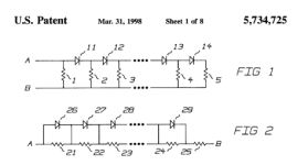
Have a look at a snippet from us patent 5734725 (1998) where a passive long sliding curve is proposed (0-NN V dc & ac; NN is gate turnoff voltage, up to 10 - 20 V, even more).
Attachments
You said in ASCII:
INPUT ---> NPN_COLLECTOR ---> OUT1 ---> GROUND
But in your drawing the emitter is connected to out1.
So, output 1 is connected to ground?
The ascii was to show the order that the components would be connected. The output of the NPN emitter could be ground or it could just complete the circuit if were not using a common ground. The drawing was intended to make things a bit clearer in that regard, and is accurate in terms of conveying the idea I have. In practical terms, both OUT1 and OUT2 would be connected to a device or to a load which requires the limited voltage.
I've tried to redraw your sketch (top) and put it in a more formal way (bottom).
So far as much you have tried to make it quite clear, with all respect, even with all other to imply other and further needed components to obtain your goal, this approach, dc or ac likewise, cannot and will not work as intended.
Setting aside voltages that would exceed the ratings of the components, why wouldn't it work in theory? What problem(s) would prevent it from working as conceptualized?
The NPN is reversed biased and does not do anything until the input voltage exceeds the Vbe breakdown at some 6V (meltdown).
The zener will only conduct ( aka do it's zener function) when there is sufficient load on out2 (unspecified), given the NPN bjt is still off.
Considering ground as an arbritairy floating ground is better considerated not as a ground, floating or not. Just to consider.
I have not taken into account any exceding parameters sofar (safe the components used in their normal operation).
But the whole concept is still not clear. The only thing I can make of it is that you want to make a 'sliding-slope' limiter, from a transistor and a zener (only, with help from some component-friends), passive and with extreme wide range covering both dc and ac.
Limiters and AGC's in general has a 'enveloping-range' (the squeezing range so to say) of some 30dB max. Your asking for zero to NN, where NN is up to 30Vdc/ac. Thats ∞dB and impossible. 1-30 Vac is already 30dB. 33mV to 1V is also 30dB. 1mV to 30mV is also 30dB.
1mV to 30V (all ac, or we're talking rubbish) is 3 * 30dB = 90dB. You need a DSP for that, but there are no passive DSP's available (yet).
With the hinted diode-resistor networks one might get some acceptable 20dB range into control, but that's it.
You have an idea. That's ok. You have an approach in mind. Great.
I'm sixty years old, being involved with electronics for 40+ years.
And I still do not understand what you try to explain.
What is, just to inquire, your 'electronics knowledge level'?
A BJT uses base current to control the flow of the collector-emitter current. That makes it an active device. That's not splitting hairs. That's applying a definition. But then again, what do I know? I only have 40+ years of hobby experience, 18 years of industry experience, and two electrical engineering degrees. I am also human and do make the occasional mistake. But I do know the difference between active and passive devices.As for the NPN requiring power to function, sure, but does it require EXTERNAL POWER.
I've labeled the terminals and the source voltage so we can talk about them without confusion.Now that I drew a diagram, is there any way you would improve my circuit so that it would work if you think that it won't work as-is?
Once Vs exceeds the zener voltage plus a diode drop the collector-base junction of the BJT will be forward biased. That's usually not what you want. The base-emitter junction will only ever get forward biased (which is what you do want if you intend to use the transistor as a switch or shunt element) if the voltage at (2) is a diode drop higher than the voltage at (1). Unless you include some resistance in series with terminal (2) you'll blow the transistor as you'll exceed the max. allowed base current pretty quickly.
What is the voltage at (1) referenced to?OUT1 (topmost): The zener will cause all of the current to flow through NPN collector to emitter as long as the voltage is below the zener voltage.
If Vs is greater than the zener voltage and (2) is taken to a potential below the negative terminal on Vs, all you'll get out of that is Vs-Vz, where Vz is the zener voltage. If you pull more current than the zener can handle you blow the zener.OUT2 (bottom): When the voltage of the source increases to the zener voltage, current will hit the base and cease to flow from the collector. Here I tapped the circuit between the zener and the base of the NPN, because this will be the "limited" voltage.
Ok, so assuming that worked you now have a circuit that either consumes gobs of power (and blows the zener) or has high output impedance. Is that what you want?While not shown here, the actual voltage coming from the zener could further be adjusted with a simple voltage divider that taps back into the wire coming out of the emitter of the NPN, with the divided voltage becoming the new OUT2.
As pointed out above, I don't see a way to get the transistor to conduct as it's reverse biased. Unless Vs can be negative that is. If it was to conduct it'll blow instantly as it would short out Vs.
Unless I'm missing something fundamental I'm just not seeing a) how this circuit would work as a limiter and b) how it would even work without blowing up. Hence, my comment earlier that it's fundamentally broken. But then again, you're leaving a lot up to the imagination here. What are the voltages at (1) and (2) referenced to? Can Vs be negative?
How about setting up the circuit in a simulator. LTspice, TINA-TI, and PSpice for TI are all free and available on the web.
A shunt regulator can be a limiter. Here's one example:
If the input voltage is below Vz+Vbe you get the input voltage across RL. Once the input voltage exceeds Vz+Vbe Q1 will conduct and limit the voltage across the load. I would add a resistor in series with the base to limit the base current.
Tom
Last edited:
- Home
- General Interest
- Everything Else
- Simplest 0 mV to NN mV Voltage Limiter