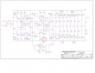
I've built this amplifier and put it in my bench to test. All the components has been inserted (as shown) except for the power transistors and the load. I wanted to check if all the voltages are correct at their nodes. After powering it up with +-12V DC, the marked resistor is getting too hot, although I've checked each and every component before assembly.
I've also rechecked the driver transistor after the initial result and replaced it but the problem persists.
What can be the reason behind this resistor getting hot without the power transistor and a load connected?
I've also rechecked the driver transistor after the initial result and replaced it but the problem persists.
What can be the reason behind this resistor getting hot without the power transistor and a load connected?
Attachments
Last edited:
Welcome to the forum!
By "except for the power transistors" are you including Q19-Q22 as well as Q24-Q35?
R34 is hot; is R40 similarly hot?
I guessing your 12V supplies are fixed so that you can't limit current or increase voltage gradually?
By "except for the power transistors" are you including Q19-Q22 as well as Q24-Q35?
R34 is hot; is R40 similarly hot?
I guessing your 12V supplies are fixed so that you can't limit current or increase voltage gradually?

Can you give us some numbers? What is the actual measured voltage across the resistor of concern.
Can you give us some numbers? What is the actual measured voltage across the resistor of concern. And is the system oscillating? (scope images)
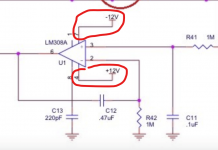
Are the collector and emitter of Q14 swapped? I assume that is intended to be a current source, but that isn't how it's connected (look at Q13 for comparison).
Nope, Q19-Q22 has been installed. R40 stays normal. Although I was trying to test using a regulated supply but, can it be the cause?Welcome to the forum!
By "except for the power transistors" are you including Q19-Q22 as well as Q24-Q35?
R34 is hot; is R40 similarly hot?
I guessing your 12V supplies are fixed so that you can't limit current or increase voltage gradually?
Thank you for the comment.
It shows an abnormal 10.8VDC. 🙁 The connected base of Q9 and Q11 is also showing 0.1V. I've checked the D5 but the zener is in good condition. I can't say about the oscillation cause I don't have a scope in my home or at least for the moment.Can you give us some numbers? What is the actual measured voltage across the resistor of concern.
Last edited:
Is the Q14 connected wrong in the schematic? I've assembled everything as shown in the diagram except for the signal input connected with R21 which I believe was a mistake in the drawing.Are the collector and emitter of Q14 swapped? I assume that is intended to be a current source, but that isn't how it's connected (look at Q13 for comparison).
It's possible that valgamaa has nailed it post 5. He's got eagle eyes!
I'm not sure how Q14 would behave if wired backwards. Its base-emitter junction might be in reverse breakdown; it would conduct heavily into Q7a, then cascade of Q9, Q15, Q17. 10.8V across the hot resistor might be about right.
Edited for typos
I'm not sure how Q14 would behave if wired backwards. Its base-emitter junction might be in reverse breakdown; it would conduct heavily into Q7a, then cascade of Q9, Q15, Q17. 10.8V across the hot resistor might be about right.
Edited for typos
Last edited:
Yes, the schematic for Q14 connection is wrong! As valgamaa noted, emitter and collector are backwards; if layout corresponds to schematic, it's likely the problem.Is the Q14 connected wrong in the schematic? I've assembled everything as shown in the diagram except for the signal input connected with R21 which I believe was a mistake in the drawing.
So in this case, swapping the collector and emitter pin of the Q14 will solve the problem, right?It's possible that valgamaa has nailed it post 5. He's got eagle eyes!
I'm not sure how Q14 would behave if wired backwards. Its base-emitter junction might be in reverse breakdown; it would conduct heavily into Q7a, then cascade of Q9, Q15, Q17. 10.7V might be about right.
Let me check and I'll keep you guyz updated. Once again, thank you for the solutions.
You've got good eyes, too! 😀---- I've assembled everything as shown in the diagram except for the signal input connected with R21 which I believe was a mistake in the drawing.
If you have no output transistors you have no real DC feedback path . Temporarily strap a 100 Ohm resistor across the base and emitter of 2 output transistors one transistor on the positive rail and another on the negative rail this will simulate the base emitter junctions , assuming you have the 0.33 Ohm emitter resistors fitted etc .
Thank you for the help. The problem got solved but a new one arrived. After measuring all the voltages I found that the base junctions of all the power transistors are showing 10.5VDC constant on both the NPN and PNP channels. I don't think it's normal but can't find out why it's happening. If I touch the input signal node and measure the AC voltage on the power BJT's base junction, it responds, but why is it showing a constant DC?Are the collector and emitter of Q14 swapped? I assume that is intended to be a current source, but that isn't how it's connected (look at Q13 for comparison).
Is this the reason I'm getting a constant DC at the base of the output transistors? Though I haven't connected any output BJTs.If you have no output transistors you have no real DC feedback path . Temporarily strap a 100 Ohm resistor across the base and emitter of 2 output transistors one transistor on the positive rail and another on the negative rail this will simulate the base emitter junctions , assuming you have the 0.33 Ohm emitter resistors fitted etc .
R26 ensures that there is no differential voltage on the differential pairs without the output transistors so this isn't necessary. When the amplifier is fully working then AC grounding this resistor would reduce the DC offset at the output and could be a worthwhile modification.If you have no output transistors you have no real DC feedback path . Temporarily strap a 100 Ohm resistor across the base and emitter of 2 output transistors one transistor on the positive rail and another on the negative rail this will simulate the base emitter junctions , assuming you have the 0.33 Ohm emitter resistors fitted etc .
To look at the output of Q17 and beyond then you will need the feedback loop to be closed, as epicyclic said. Even so, the base voltages of the NPN transistors and PNP ones shouldn't be the same.Is this the reason I'm getting a constant DC at the base of the output transistors? Though I haven't connected any output BJTs.
With the power off, measure the resistance of R24, to be sure it isn't open-circuit after the overheating earlier. Is there around 0.7 volts between the base and emitter of Q17? If these are both OK then Q17 should be sinking current and there should be a voltage drop across Q23 collector and emitter. This should supply the offset needed between the PNP and NPN output transistors, when you add them.
Assuming only Q19-Q22 are present, my suggestion would be to temporarily connect the "output" buss of all those 0.33 ohm resistors to the emitter of Q19. This will provide a feedback connection to R27. Set R43 for minimum resistance.
Power with those dual 12V supplies. (There may be oscillation because the R48 + C14 network is intended to be driven from the output transistors. If it becomes troublesome, we'll find a work-around.) With any luck, the emitter of Q19 will bias to about 0V, and the emitter of Q22 will be about +1.8V. The opamp is a "DC servo" that is intended to drive output voltage to 0V. It may not work due to other issues, so let me know what you observe.
Power with those dual 12V supplies. (There may be oscillation because the R48 + C14 network is intended to be driven from the output transistors. If it becomes troublesome, we'll find a work-around.) With any luck, the emitter of Q19 will bias to about 0V, and the emitter of Q22 will be about +1.8V. The opamp is a "DC servo" that is intended to drive output voltage to 0V. It may not work due to other issues, so let me know what you observe.
Yep, the conditions are good. All the resistors, including R24, are showing resistance and I'm getting 0.52 volts between the base emitter of Q17. So it's okay to put the power transistors for further inspection, right?To look at the output of Q17 and beyond then you will need the feedback loop to be closed, as epicyclic said. Even so, the base voltages of the NPN transistors and PNP ones shouldn't be the same.
With the power off, measure the resistance of R24, to be sure it isn't open-circuit after the overheating earlier. Is there around 0.7 volts between the base and emitter of Q17? If these are both OK then Q17 should be sinking current and there should be a voltage drop across Q23 collector and emitter. This should supply the offset needed between the PNP and NPN output transistors, when you add them.
- Home
- Amplifiers
- Solid State
- Aragon 8008 troubleshooting