Yep. That’s just a standard galaxy, probably the smallest one. 230x170 I think… I’ll measure when I get home.
https://diyaudiostore.com/collections/galaxy/products/galaxy-1u-w-steel-covers?variant=12174717508
https://diyaudiostore.com/collections/galaxy/products/galaxy-1u-w-steel-covers?variant=12174717508
Patrick, OT to this circuit, but how do you put .op labels on an LTSpice schematic that show current? I've given up from searching. Thanks.
30 seconds in google :
https://electronics.stackexchange.c...ow-can-i-display-the-current-in-the-schematic
Patrick

Any idea when the kits will be in the store?
Shipped to the store last week.


I need to learn to dumb down my searches. Terms like "op data label current," even at ADI and the Wiki page, didn't find that. Thanks!
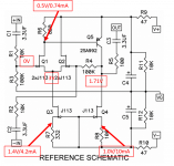
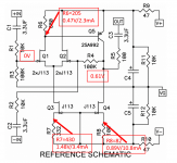
Offset at the output, need help. I put all measured voltage and current on the schematics.
J113 has a Idss around 25mA, Q1 and Q2 are matched to 0.01mA at 25.5V Vds and 1.5mA. All other components are exactly as in the picture. I don't know if it is normal.
Power supply +/-24VDC
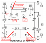
J113 has a Idss around 25mA, Q1 and Q2 are matched to 0.01mA at 25.5V Vds and 1.5mA. All other components are exactly as in the picture. I don't know if it is normal.
Power supply +/-24VDC
Attachments
In order to drop the presented voltage to the FE2022. Would raising R9 and or R10 (depending on set-up) be the correct method ? Or would this cause negative results ?
Thanks! Zen Mod!
Did you mean to reduce R6 or increase R7?
if DC Offset is positive, that means upper part of OS is more open than lower one
so, there is too much voltage sag across R6
to decrease that voltage, you need to decrease current through LTP
to do that, you need to vary R7 ....... to decrease current, you must increase R7
replace R7 with 270R fixed resistor in series with 100R trimpot, so effective R7 value can be set between 270R to 370R
or leave 330R in situ, add 50R trimpot in series
changed R6 to 206 and R7 to 360, the offset is now 0.85V.
so we are moving in the correct direction?
so we are moving in the correct direction?
Attachments
Last edited:
Could we increase the current of the VAS stage to compensate +offset?if DC Offset is positive, that means upper part of OS is more open than lower one
so, there is too much voltage sag across R6
..................................
Say we could parallel the Q4?
Maybe not. Q5 cannot handle it.
If we could change to a TO220 Q5?
Last edited:
Could we increase the current of the VAS stage to compensate +offset?
one can do whatever he want ..... but best from position of someone not needing to ask question as above .......
so, wise to keep OLG figure as Pa arranged it and make changes without messing with same
as I wrote before in this very thread - if you want bigger and sturdier FE stage, go build another one; plenty to choose from, new Stasis FE being first but certainly not only one
changed R6 to 206 and R7 to 360, the offset is now 0.85V.
so we are moving in the correct direction?
something is fishy
describe PSU arrangement, and do you have prescribed semis, all of them?
best to leave R6 as is, reason mentioned up
increase R7 as much is needed, to get prescribed sum Iq for LTP, aroundish 2mA
I have done this in the past. Slightly dangly but it works.replace R7 with 270R fixed resistor in series with 100R trimpot,
https://www.diyaudio.com/community/...sfet-muff-and-defisit-amplifier.392733/page-3
The DC-DC SMPS.
Everything follows Pass FE2022. All semis. KSA992FBTA, J113. The first stage pair uses only single 1xJ113 not 2xJ113.
The DC-DC SMPS.
Everything follows Pass FE2022. All semis. KSA992FBTA, J113. The first stage pair uses only single 1xJ113 not 2xJ113.
Attachments
again, leave R6 as original
when I (unfortunately) mention it, I meant just slight change, not so drastic one; so, best to leave it original, and keep increasing R7 value until you get proper DC offset
in general:
in case of bipolar supply, proper DC offset means 0mV-ish (your case, dual rails, as per link you posted)
in case of single rail supply, then output node must be near rail/2, and we must keep/use output coupling cap
everything as Pa already described
- Home
- Amplifiers
- Pass Labs
- DIY Front End 2022