Hi all,
... & thanks for your various replies - I will try to comment in sequence below ...
@Markw4 :
Yes, that is also my understanding and what I actually hinted at in the first section of post #15. However, I assume (and I say assume because I am not able to calculate what would be the required resolution here) that using an oscilloscope is not sufficient to reveal the reflections that may be relevant in audio contexts? As I understand it most of the measurement processes have an offspring in data transmission contexts - i.e. ensuring data/signal integrity - which I reckon is insufficient when one starts investigating femtosecond time variations ... right/not entirely right ... ?
Maybe this also applies to TDR measurements which may show impedance variations - but unless it is maybe expensive equipment will it then show low-level impedance variations that may cause femtosecond timing errors that may be relevant in audio? Asking not rhetorically, but because I don't know ...
Hmmm ... this is an interesting comment - and I admittedly am not that knowledgeable in this field - but if I understand Eric Bogatin correctly: even when the signal line is short relative to the rise time there will be "like waves" on the signal voltage - something that, if correct, I reckon would affect the timing of the DAC/ADC triggering. I can link to an example of this is someone is interested ...
@bohrok2610 :
@tomchr : Well ... first a complete digression: I remember a couple of months ago - probably as stray-thoughts - to have wondered whether "at skyde sig selv i foden" - as it is called in Danish - would have a parallel in English ... And reading your post apparently it has ("shoot yourself in the foot") - well, learning sometimes has its unforeseen ways 😉
Regarding your interesting comments I can say that, yes, the example in Post #1 shows vias connected to an underlying GND plane.
Well, I have found somewhat contradictory information about the effect of via stitching in my searches, yet:
- if you look at the short video clip in #1 it is shown that having a via stitching along a trace has a quite profound effect on the EMR from a given trace. When the trace is lined with the vias the radiation appears to be significantly reduced. However, Eric Bogatin and Seminovich (I think his name is?) in the article linked to in #1 found that via stitching only reduces radiation by some 30-50% with a microstrip trace (under various conditions). For a stripline OTOH the radiation attenuation is very efficient.
- The article that I linked to in #13 shows the effect of these via stitches when varying via interdistance and closeness to the trace (from p. 12). A bit surprisingly (to me) is that they found that placing the vias close to the trace visibly improves bandwidth linearity. Also it is shown that really reducing the inter-via distance significantly impacts higher frequency linearity (above 1 GHz - but probably sensible with some margin here ... ?).
I think you are right about this but I would like to be able to quantify the impedance change. But maybe it is insignificant: E.g. in the article linked to in #13 there is no mentioning of an impedance change when they conduct their trials of inter-via spacing and distances towards the trace. So maybe a change on the order of 1/100th the impedance of the trace itself .. ??
Very interesting observation, Tom. I have not read about this effect elsewhere - any chance you can elaborate a bit on why this should be the case? Personally, I would expect a closely "peppered" Signal/GND layered PCB to have an intrisically quite linear frequency response and also to be quite electrically well-defined relative to its on-board components & external EMR ... But why a higher impedance ... ?
On the other hand I did notice that Eric Bogatin in one of Robert Feranec's videos showed an Arduino One PCB layout that had been made in one of his PCB design classes where there wasn't a GND pour on the top plane .. only the signal & power traces atop a GND plane. Which surprised me - thinking that it might somehow relate to your observation?
Thanks again for your comments. I admittedly find this to be a very interesting field so I appreciate your insights!
Cheers, Jesper
... & thanks for your various replies - I will try to comment in sequence below ...
@Markw4 :
That's because the 100R resistor causes reflections too. The more it looks like a lump of Z on the line that does not match the line Z, the more energy will be reflected.
Yes, that is also my understanding and what I actually hinted at in the first section of post #15. However, I assume (and I say assume because I am not able to calculate what would be the required resolution here) that using an oscilloscope is not sufficient to reveal the reflections that may be relevant in audio contexts? As I understand it most of the measurement processes have an offspring in data transmission contexts - i.e. ensuring data/signal integrity - which I reckon is insufficient when one starts investigating femtosecond time variations ... right/not entirely right ... ?
Maybe this also applies to TDR measurements which may show impedance variations - but unless it is maybe expensive equipment will it then show low-level impedance variations that may cause femtosecond timing errors that may be relevant in audio? Asking not rhetorically, but because I don't know ...
The lines we might want to damp between the last reclocker and the dac chip are usually fairly short in that respect. In that case we wouldn't expect to see much in the way of significant mismatch reflections.
Hmmm ... this is an interesting comment - and I admittedly am not that knowledgeable in this field - but if I understand Eric Bogatin correctly: even when the signal line is short relative to the rise time there will be "like waves" on the signal voltage - something that, if correct, I reckon would affect the timing of the DAC/ADC triggering. I can link to an example of this is someone is interested ...
@bohrok2610 :
I agree - yet I know I will not be able to do so in all cases due to lack of knowledge of correct terminology. If you comment on my posts I hope I can ask you to bear with me.BTW it is better to use proper terminology (i.e. series termination resistor, not damping resistor) as it helps in finding resources.
@tomchr : Well ... first a complete digression: I remember a couple of months ago - probably as stray-thoughts - to have wondered whether "at skyde sig selv i foden" - as it is called in Danish - would have a parallel in English ... And reading your post apparently it has ("shoot yourself in the foot") - well, learning sometimes has its unforeseen ways 😉
Regarding your interesting comments I can say that, yes, the example in Post #1 shows vias connected to an underlying GND plane.
I doubt it's much, though, as the distance from the traces to the vias (think 3D through the prepreg) is pretty long relative to the space from the traces to the ground plane (or between traces).
Well, I have found somewhat contradictory information about the effect of via stitching in my searches, yet:
- if you look at the short video clip in #1 it is shown that having a via stitching along a trace has a quite profound effect on the EMR from a given trace. When the trace is lined with the vias the radiation appears to be significantly reduced. However, Eric Bogatin and Seminovich (I think his name is?) in the article linked to in #1 found that via stitching only reduces radiation by some 30-50% with a microstrip trace (under various conditions). For a stripline OTOH the radiation attenuation is very efficient.
- The article that I linked to in #13 shows the effect of these via stitches when varying via interdistance and closeness to the trace (from p. 12). A bit surprisingly (to me) is that they found that placing the vias close to the trace visibly improves bandwidth linearity. Also it is shown that really reducing the inter-via distance significantly impacts higher frequency linearity (above 1 GHz - but probably sensible with some margin here ... ?).
I doubt it's much, though,
I think you are right about this but I would like to be able to quantify the impedance change. But maybe it is insignificant: E.g. in the article linked to in #13 there is no mentioning of an impedance change when they conduct their trials of inter-via spacing and distances towards the trace. So maybe a change on the order of 1/100th the impedance of the trace itself .. ??
I have a sneaky suspicion that they end up shooting themselves in the foot that way as it increases the ground impedance rather than lowering it.
Very interesting observation, Tom. I have not read about this effect elsewhere - any chance you can elaborate a bit on why this should be the case? Personally, I would expect a closely "peppered" Signal/GND layered PCB to have an intrisically quite linear frequency response and also to be quite electrically well-defined relative to its on-board components & external EMR ... But why a higher impedance ... ?
On the other hand I did notice that Eric Bogatin in one of Robert Feranec's videos showed an Arduino One PCB layout that had been made in one of his PCB design classes where there wasn't a GND pour on the top plane .. only the signal & power traces atop a GND plane. Which surprised me - thinking that it might somehow relate to your observation?
Thanks again for your comments. I admittedly find this to be a very interesting field so I appreciate your insights!
Cheers, Jesper
With 200MHz oscilloscope you should be able to tune the over/undershoots of I2S/PCM/DSD lines with series termination resistors. Minor overshoots are not an issue but large overshoots may cause sampling errors and induce ground bounce.Yes, that is also my understanding and what I actually hinted at in the first section of post #15. However, I assume (and I say assume because I am not able to calculate what would be the required resolution here) that using an oscilloscope is not sufficient to reveal the reflections that may be relevant in audio contexts?
Jesper,
Yes, even with short lines in reality there are always reflections.
However, I think all the focus on vias is a diversion from what the real problems with clocking are and how they arise. The whole story, or as much of it as know about at this point, is rather complicated. As Chris719 pointed out in the posts I linked, series termination isn't used when signal integrity is of the utmost importance (i.e. lowest possible jitter). In fact the clocks, FIFO buffer, discrete resistor dac designed by Andrea Mori all use parallel termination at the receiving end because it is closer to ideal. I have one of those dac systems here and we have compared the sound with my AK4499 dac (which is unconventional, not pure textbook). The two dacs a bit sound different, but overall SQ is about the same. For example, Andrea's dac sounds a little better at LF, and the AK4499 sounds a little better at HF. The reason that can be the case is because of the some of the partially non-textbook solutions used in the AK4499 dac.
Regarding the focus on ideal line damping, it doesn't appear the be the biggest problem with clocking. Perhaps consider that a dac clock input is level sensitive. It doesn't switch based on the exact shape of the arriving pulse. It switches when the receiver switching threshold voltage is crossed. A fast risetime as the pulse passes though the receiver threshold voltage window helps to keep amplitude noise in the receiver from introducing its own timing errors (jitter/phase noise). (Even that explanation is somewhat simplfied.) However, a fast risetime can couple GHz noise into the dac substrate. There is always some tradeoff.
IME most of the problems with jitter and or close-in phase noise arise in the circuitry that launches a clock pulse down the transmission line, how that circuitry is powered and bypassed, and how clean the ground is where that circuitry is located. By focusing attention on those things I can get almost as the same SQ using Crystek clocks as by using exotic SOA or near SOA clocks. And I can get nearly the same SQ using distributed damping as I can get using more ideal transmission lines and parallel termination. But, as Syn08 found out, relative timing of signals can matter (I2S and clock signals, in this case), but the datasheet doesn't always tell you about it. It can be as important or more important as the getting lowest possible jitter.
Regarding focus on phase noise numbers expressed in fs, we are talking about averaged phase noise per offset frequency, not peak phase noise, not the time domain waveform showing phase variation over time. Why? Its just like our focus on steady state harmonic distortion. Its because its reasonably practical to measure, not because its exactly what we should really want to know.
To sum it up, focusing on this and that thing, such as vias, such as bypass caps, as though they are isolated from each other and each one can be individually optimized is sort of a product of Western culture thinking where we tend see things as discrete objects, rather than as a whole where the relationship between objects is as important or more important than the objects themselves. Maybe like focusing on individual trees instead of seeing a forest that is actually more than a set of trees. Its a whole interactive ecology.
Last edited:
An opinion:
Regarding looking at clock pulse waveshape with a scope, IMHO a low capacitance active probe is mandatory. Passive 10x scope probe capacitance can be enough to cause reflections and distort the waveform. Lacking an active probe, using a diy low capacitance probe may be the next best thing: http://jahonen.kapsi.fi/Electronics/DIY 1k probe/
Regarding looking at clock pulse waveshape with a scope, IMHO a low capacitance active probe is mandatory. Passive 10x scope probe capacitance can be enough to cause reflections and distort the waveform. Lacking an active probe, using a diy low capacitance probe may be the next best thing: http://jahonen.kapsi.fi/Electronics/DIY 1k probe/
Last edited:
As a friendly reminder when you link to posts made by others do not add your own interpretations. Chris719 did not mention jitter in his posts.As Chris719 pointed out in the posts I linked, series termination isn't used when signal integrity is of the utmost importance (i.e. lowest possible jitter).
Last edited:
To quote means to enclose exact words in quote marks "like this." What I did was reference another source of information. A reference and a quote may or may not be the same thing. In most cases a reference is not a literal quote.
Other than that, signal integrity is a broad term that can include jitter.
I will not comment further on this issue for now.
Other than that, signal integrity is a broad term that can include jitter.
I will not comment further on this issue for now.
Last edited:
IME noise on Vref can easily add much more close-in phase noise than even a poor clock. It is possible for the diyer to make basic analyses of the close-in phase noise using very large FFT size: https://www.diyaudio.com/community/threads/phase-noise-in-ds-dacs.387862/IME most of the problems with jitter and or close-in phase noise arise in the circuitry that launches a clock pulse down the transmission line, how that circuitry is powered and bypassed, and how clean the ground is where that circuitry is located.
Thank you for your comment.
My understanding would be that Vref noise is amplitude noise, not phase noise. It still appears as FFT skirts because the amplitude noise more or less creates new frequency components that are closely correlated with the test tone.
Perhaps Marcel would care to comment?
My understanding would be that Vref noise is amplitude noise, not phase noise. It still appears as FFT skirts because the amplitude noise more or less creates new frequency components that are closely correlated with the test tone.
Perhaps Marcel would care to comment?
Terminology-wise you are correct. But the FFT noise skirts are a composite of various low frequency noises. These have impact on dac performance whether or not the low frequency noises originate from clock or from Vref.
Regarding terminology this recent paper divides phase noise into PM noise and AM noise.
https://hal.archives-ouvertes.fr/hal-02370697/document
https://hal.archives-ouvertes.fr/hal-02370697/document
Attached is a Crystek app note which addresses the two types of clock oscillator noise.
IMHO clock amplitude noise could, for example, potentially affect the edge timing of some clock squaring circuits and thus affect jitter.
However, it seems to me the mechanism of Vref noise does not affect jitter in the same way.
IMHO clock amplitude noise could, for example, potentially affect the edge timing of some clock squaring circuits and thus affect jitter.
However, it seems to me the mechanism of Vref noise does not affect jitter in the same way.
Attachments
Last edited:
Jitter relates to clocks not dac output. It is not possible to make judgements about dac quality based on the clock alone.
According to the information linked to in this post https://www.diyaudio.com/community/threads/phase-noise-in-ds-dacs.387862/post-7066124 close-in amplitude noise tends to be more audible than close-in phase noise at frequency offsets below 90 Hz from a 1 kHz carrier. Anyway, both are off topic.
Hej Jesper,
Mvh,
Tom
That could be. I was thinking about the impedance of the lines and not so much from an EMI perspective. I would think (and this is just hand waving) that a better RF ground near the traces would terminate any stray EM field lines better, thus, result in lower EM radiation. That part does make sense.- if you look at the short video clip in #1 it is shown that having a via stitching along a trace has a quite profound effect on the EMR from a given trace. When the trace is lined with the vias the radiation appears to be significantly reduced. However, Eric Bogatin and Seminovich (I think his name is?) in the article linked to in #1 found that via stitching only reduces radiation by some 30-50% with a microstrip trace (under various conditions). For a stripline OTOH the radiation attenuation is very efficient.
That also makes sense. The largest standing wave you can support with a stitched plane would have a node at each via. So the stitching would lose its effectiveness once the wavelength of the operating frequency approaches twice the distance between the vias.Also it is shown that really reducing the inter-via distance significantly impacts higher frequency linearity (above 1 GHz - but probably sensible with some margin here ... ?).
I've seen a couple of examples scattered on this forum where people would place lots and lots of vias on ground planes and pours intended to conduct high current at audio frequencies. Visualize a via matrix covering the entire plane/pour where the vias are placed together as close as possible. I'm guessing the thought was that the metal in the vias would help lowering the DC resistance. The issue is that each via removes a good chunk of the relatively thick (35 um) copper and replaces it with a pretty skinny tube of electroplated gold. Typically the wall thickness of a via is around 0.5 mil (=12.7 um). As long as we're talking DC (or audio frequencies) they'd be better off stitching the planes/pours on the ends only.Very interesting observation, Tom. I have not read about this effect elsewhere - any chance you can elaborate a bit on why this should be the case? Personally, I would expect a closely "peppered" Signal/GND layered PCB to have an intrisically quite linear frequency response and also to be quite electrically well-defined relative to its on-board components & external EMR ... But why a higher impedance ... ?
Mvh,
Tom
Hi all,
Pleased to see so many comments & interesting insights 😉 ...
@bohrok2610 :
@Markw4 :
On the other hand I have noticed that e.g. the Soekris DAM 1021 uses thevenin terminations with a coupling capacitor in-between, thus: transmitter IC-capacitor-thevenin resistors-receiving end. I reckon this arrangement may have two advantages: It may achieve the advantages of a thevenin termination (no first reflection), yet also prevent LF/DC power from spreading to the individual parts of the PCB. However - any thoughts on adding the capacitor in terms of jitter, anyone?
@tomchr : Hej Tom (still a Dane in the US I suppose?) - & thank you for clarifying.
I reckon that overall it is a question of discernment as to which choices to make in a given situation. Life
@MarcelvdG : Thank you also for chiming in, Marcel. Interesting information (hearing amplitude modulation) in relation to e.g. Vrefs or Vcc voltages on ICs.
And then, not intending to end any further exchange here, but I think that the subject I originally posted about - the lining vias - have been touched upon to a fair extent so I personally do not need more feedback on this. Thanks again to you all for considering & replying.
Cheers,
Jesper
Pleased to see so many comments & interesting insights 😉 ...
@bohrok2610 :
Hmmm... I will consider trying it out and see if I get meaningful results.With 200MHz oscilloscope you should be able to tune the over/undershoots of I2S/PCM/DSD lines with series termination resistors. Minor overshoots are not an issue but large overshoots may cause sampling errors and induce ground bounce.
Interesting measurements ... Not that often that the direct effect of a component change is this obvious. And although I do notice that the difference between the two oscillators is not huge I also notice that the skirts of the NZ2520SDA fall off more rapidly than the other oscillator.IME noise on Vref can easily add much more close-in phase noise than even a poor clock. It is possible for the diyer to make basic analyses of the close-in phase noise using very large FFT size: https://www.diyaudio.com/community/threads/phase-noise-in-ds-dacs.387862/
@Markw4 :
.. Are you sure about this, Mark? When looking at the picture of the Lite DAC in the DAC's user manual it doesn't look as if it is parallel termination - no resitors present as far as I can see at the receiving end of the clock lines for example. Also, as far as I understand Eric Bogatin series termination can be just as feasible if the impedances at the transmitting end & the trace are carefully matched. In this case the transmitting end (driver output impedance + series termination resistor) fully attenuate the reflected signal from the receiving end. So I assume it depends on the clock frequency - whether or not there is time to allow for a double transmission delay period ...In fact the clocks, FIFO buffer, discrete resistor dac designed by Andrea Mori all use parallel termination at the receiving end because it is closer to ideal.
On the other hand I have noticed that e.g. the Soekris DAM 1021 uses thevenin terminations with a coupling capacitor in-between, thus: transmitter IC-capacitor-thevenin resistors-receiving end. I reckon this arrangement may have two advantages: It may achieve the advantages of a thevenin termination (no first reflection), yet also prevent LF/DC power from spreading to the individual parts of the PCB. However - any thoughts on adding the capacitor in terms of jitter, anyone?
I tend to agree although I have not yet had the chance to actually listen to the differences (I also don't have suitable measurement equipment, unfortunately). I hope to do so in not too long.IME most of the problems with jitter and or close-in phase noise arise in the circuitry that launches a clock pulse down the transmission line, how that circuitry is powered and bypassed, and how clean the ground is where that circuitry is located.
This is a side remark that I do not intend to follow-up, but since you mentioned it: I tend to see it as if optimizing various parts of a whole allows the whole to be lifted to a higher level, so to speak. On the other hand if any individual part is not just reasonably optimized it may be a challenge to make the whole achieve high quality. Thus my interest in the stitching vias and their impedance, because I did not know to which extent an impedance mismatch here might influence the whole.To sum it up, focusing on this and that thing, such as vias, such as bypass caps, as though they are isolated from each other and each one can be individually optimized is sort of a product of Western culture thinking where we tend see things as discrete objects, rather than as a whole where the relationship between objects is as important or more important than the objects themselves.
Assuming that your suggestion is made for me I can say that I have an appr. 0.2pF, 1GHz probe.IMHO a low capacitance active probe is mandatory.
@tomchr : Hej Tom (still a Dane in the US I suppose?) - & thank you for clarifying.
Ah, I see what you mean. I actually thought that a via's wall thickness was thicker - 12.5 um is not a lot if one is e.g. trying to carry some current (or maybe would like low impedances for some reason).The issue is that each via removes a good chunk of the relatively thick (35 um) copper and replaces it with a pretty skinny tube of electroplated gold. Typically the wall thickness of a via is around 0.5 mil (=12.7 um). As long as we're talking DC (or audio frequencies) they'd be better off stitching the planes/pours on the ends only.
I reckon that overall it is a question of discernment as to which choices to make in a given situation. Life
@MarcelvdG : Thank you also for chiming in, Marcel. Interesting information (hearing amplitude modulation) in relation to e.g. Vrefs or Vcc voltages on ICs.
And then, not intending to end any further exchange here, but I think that the subject I originally posted about - the lining vias - have been touched upon to a fair extent so I personally do not need more feedback on this. Thanks again to you all for considering & replying.
Cheers,
Jesper
Not sure where you are looking on the pic. So far as I know the only termination Andrea considers valid is parallel... Are you sure about this, Mark?
Assuming that your suggestion is made for me I can say that I have an appr. 0.2pF, 1GHz probe.
It was a general comment about scoping clocks is all. Good to know you have one though.
Hi all,
... reviving an old thread which touches upon a subject that continues to puzzle me: The effects of vias in a PCB.
As it is I have for some time now been wondering about the effect of through-GND-stitching-vias (TGSV onwards), i.e. GND vias going all the way through the PCB, on the shielding effectiveness of the PCB copper layers between the top and the bottom sides of the PCB. That is: How much is the shielding between the top layer and the bottom layer of e.g. a 4 layer PCB deteriorated by adding (many) GND through-vias / stitching vias to the PCB?
I have searched the internet for this information but have not really found anything specific (and ChatGPT was ambiguous in its replies ) so I hope one of you may know about this ...
I reckon there are many factors to consider:
- The resonance frequency of the via(s) and attenuation per decade away from this frequency. If e.g. the resonance frequency of a TGSV is 10 GHz how much is the "conduction attenation" of such a via per decade? E.g. how much will a 100 MHz top layer signal passing through this via to the bottom layer be attenuated? Is it 20 dB per decade (or ?) ... or does some other phenomenon come into play here?
- The path of least inductance/impedance. I reckon that due to the return currents moving along the path of least inductance/impedance most of the return currents going through a TGSV will mainly move between the relevant/nearest layers of the PCB. Thus a top layer component's return current(s) will mainly move on the layer below the component (typically a GND layer). But I guess just a tiny bit of this return current may end up at the bottom layer (due to non-zero inductances & impedances of the involved vias and planes) - here potentially causing some radiation - anyone knows about the level of such radiation?
And then an additional via related question: How much does a signal through-via - e.g. connecting a trace between layers 1 & 3 (but ending on layer 4) - radiate on layer 4, i.e. the "via stub"-end-layer?
I realize that these likely are very specific questions but just in case someone knows I would appreciate your feedback (a link(s) to not too technical articles or internet pages would also be appreciated).
Cheers & thanks,
Jesper
... reviving an old thread which touches upon a subject that continues to puzzle me: The effects of vias in a PCB.
As it is I have for some time now been wondering about the effect of through-GND-stitching-vias (TGSV onwards), i.e. GND vias going all the way through the PCB, on the shielding effectiveness of the PCB copper layers between the top and the bottom sides of the PCB. That is: How much is the shielding between the top layer and the bottom layer of e.g. a 4 layer PCB deteriorated by adding (many) GND through-vias / stitching vias to the PCB?
I have searched the internet for this information but have not really found anything specific (and ChatGPT was ambiguous in its replies
) so I hope one of you may know about this ...I reckon there are many factors to consider:
- The resonance frequency of the via(s) and attenuation per decade away from this frequency. If e.g. the resonance frequency of a TGSV is 10 GHz how much is the "conduction attenation" of such a via per decade? E.g. how much will a 100 MHz top layer signal passing through this via to the bottom layer be attenuated? Is it 20 dB per decade (or ?) ... or does some other phenomenon come into play here?
- The path of least inductance/impedance. I reckon that due to the return currents moving along the path of least inductance/impedance most of the return currents going through a TGSV will mainly move between the relevant/nearest layers of the PCB. Thus a top layer component's return current(s) will mainly move on the layer below the component (typically a GND layer). But I guess just a tiny bit of this return current may end up at the bottom layer (due to non-zero inductances & impedances of the involved vias and planes) - here potentially causing some radiation - anyone knows about the level of such radiation?
And then an additional via related question: How much does a signal through-via - e.g. connecting a trace between layers 1 & 3 (but ending on layer 4) - radiate on layer 4, i.e. the "via stub"-end-layer?
I realize that these likely are very specific questions but just in case someone knows I would appreciate your feedback (a link(s) to not too technical articles or internet pages would also be appreciated).
Cheers & thanks,
Jesper
Not one bit, assuming that the via barrel is properly plated. In that case, the top plane is directly connected to the bottom plane by copper tubes. And anything between those two planes is contained by the shield. The limit will be the via spacing and dielectric constant of the pcb, which determines the upper frequency limit at which the shield loses effectivenessAs it is I have for some time now been wondering about the effect of through-GND-stitching-vias (TGSV onwards), i.e. GND vias going all the way through the PCB, on the shielding effectiveness of the PCB copper layers between the top and the bottom sides of the PCB. That is: How much is the shielding between the top layer and the bottom layer of e.g. a 4 layer PCB deteriorated by adding (many) GND through-vias / stitching vias to the PCB?
It would help you, and anyone watching, if you made a drawing of what you are thinking if. Even a rough hand drawn one.
Hi VivaVee,
& many thanks for your feedback 😉 ... (which surprisingly essentially is exactly opposite to what ChatGPT replied ...)
Anyway, here's a screen-dump of part of the layout that I am working on (a variant of MarcelvdG's FIRDAC) - as you can see there are some through-vias connecting the planes.
Hmmm ... it would be interesting to know what the relationship is between these parameters. I remember Rick Hartley (reknowned PCB designer, I think) said that 15mm spacing between vias is sufficient for a 1 GHz "efficiency" - but would you happen to have a formula (or maybe a link to such information?).
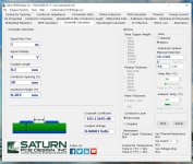
Typically, the via distance on the PCB in question is 2.5mm and the Dk of the PCB is 4.4. PCB thickness is 0.8mm and the copper layer thickness is 35um on each layer. Vias are 0.3mm hole size and the copper cladding is appr. 18 um.
BTW - since you appear to know about these things - would you happen to have a guideline for how much a stub via radiates (second part of my post above):
I have considered this using the crosstalk calculator in Saturn's PCB design toolkit but I am not sure it is applicable to this context (pls see attachment 2) ...
Cheers,
Jesper
& many thanks for your feedback 😉 ... (which surprisingly essentially is exactly opposite to what ChatGPT replied ...)
Anyway, here's a screen-dump of part of the layout that I am working on (a variant of MarcelvdG's FIRDAC) - as you can see there are some through-vias connecting the planes.
The limit will be the via spacing and dielectric constant of the pcb, which determines the upper frequency limit at which the shield loses effectiveness
Hmmm ... it would be interesting to know what the relationship is between these parameters. I remember Rick Hartley (reknowned PCB designer, I think) said that 15mm spacing between vias is sufficient for a 1 GHz "efficiency" - but would you happen to have a formula (or maybe a link to such information?).
Typically, the via distance on the PCB in question is 2.5mm and the Dk of the PCB is 4.4. PCB thickness is 0.8mm and the copper layer thickness is 35um on each layer. Vias are 0.3mm hole size and the copper cladding is appr. 18 um.
BTW - since you appear to know about these things - would you happen to have a guideline for how much a stub via radiates (second part of my post above):
And then an additional via related question: How much does a signal through-via - e.g. connecting a trace between layers 1 & 3 (but ending on layer 4) - radiate on layer 4, i.e. the "via stub"-end-layer?
I have considered this using the crosstalk calculator in Saturn's PCB design toolkit but I am not sure it is applicable to this context (pls see attachment 2) ...
Cheers,
Jesper
Attachments
- Home
- Source & Line
- Digital Line Level
- Vias lining a PCB trace - how do they change trace impedance? .. & crosstalk ...?