Hi!
I have a problem with the Audison amplifier. I don't know why it doesn't come out of "safe" mode. I was wondering if the problem was with the power supply or the amplifier. I pulled out 4 rectifier diodes, but the problem persists, it seems to me that it is somewhere in the power section, but I can't find anything. There was a bit of cold solder which I tweaked, but the problem persists.
All measurements were made at a voltage of 13.50V relative to the "-BATT" (power ground).
I think the SG2525AP is broken, but i'm not sure.
SG2525AP
P1 - 2,21V
P2 - 2,66V
P3 - 0.00V
P4 - 0.38V
P5 - 2.02V
P6 - 3.84V
P7 - 1.96V
P8 - 0.30V
P9 - 6.00V
P10 - 3.98V
P11 - 0.00V
P12 - GND
P13 - 13,48V
P14 - 0,00V
P15 - 13,44V
P16 - 5,18V
BA10393 (dual comparator)
P1 - 12,56V
P2 - 2,26V
P3 - 11,31V
P4 - GND
P5 - 12,57V
P6 - 11,31V
P7 - 13,39V
P8 - 13,44V
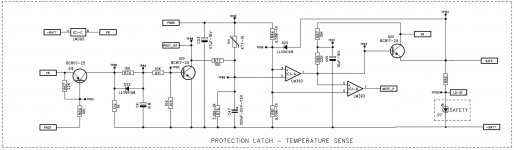
The schematic screenshots that I added in the attachment are from the LRX 1.400 model (follow the zippyshare link for the complete schematic), which is a monoblock.
The protect section is the same.
Unfortunately, I did not find the LRX 4.300.
https://www30.zippyshare.com/v/5PGBR9Mm/file.html
I have a problem with the Audison amplifier. I don't know why it doesn't come out of "safe" mode. I was wondering if the problem was with the power supply or the amplifier. I pulled out 4 rectifier diodes, but the problem persists, it seems to me that it is somewhere in the power section, but I can't find anything. There was a bit of cold solder which I tweaked, but the problem persists.
All measurements were made at a voltage of 13.50V relative to the "-BATT" (power ground).
I think the SG2525AP is broken, but i'm not sure.
SG2525AP
P1 - 2,21V
P2 - 2,66V
P3 - 0.00V
P4 - 0.38V
P5 - 2.02V
P6 - 3.84V
P7 - 1.96V
P8 - 0.30V
P9 - 6.00V
P10 - 3.98V
P11 - 0.00V
P12 - GND
P13 - 13,48V
P14 - 0,00V
P15 - 13,44V
P16 - 5,18V
BA10393 (dual comparator)
P1 - 12,56V
P2 - 2,26V
P3 - 11,31V
P4 - GND
P5 - 12,57V
P6 - 11,31V
P7 - 13,39V
P8 - 13,44V
The schematic screenshots that I added in the attachment are from the LRX 1.400 model (follow the zippyshare link for the complete schematic), which is a monoblock.
The protect section is the same.
Unfortunately, I did not find the LRX 4.300.
https://www30.zippyshare.com/v/5PGBR9Mm/file.html
Attachments


Thanks for reply Perry. 🙂
Unfortunately, nothing has changed. Is the voltage ok 4V on pin no. 10 is correct? I do not know if there should be a voltage close to the supply voltage, or should it be lower than 4V.
The Q23 emitter is about 12V and the R61 (10kohm) resistor lowers it to 4V and then enters pin 10 of the SG2525AP chip.
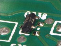
There was moisture on the collector of transistor Q23, also on pins 1 and 2 of the comparator, I removed the moisture, the pad under the collector fell off the PCB, but I soldered it higher (enlarge photo), I checked the transitions between the elements and I did not see anything suspicious. That's why my post on the forum, because I don't know what to do next - I'm out of ideas. 🙁
Unfortunately, nothing has changed. Is the voltage ok 4V on pin no. 10 is correct? I do not know if there should be a voltage close to the supply voltage, or should it be lower than 4V.
The Q23 emitter is about 12V and the R61 (10kohm) resistor lowers it to 4V and then enters pin 10 of the SG2525AP chip.
There was moisture on the collector of transistor Q23, also on pins 1 and 2 of the comparator, I removed the moisture, the pad under the collector fell off the PCB, but I soldered it higher (enlarge photo), I checked the transitions between the elements and I did not see anything suspicious. That's why my post on the forum, because I don't know what to do next - I'm out of ideas. 🙁
Attachments

Last edited:
Yes, the only difference is a slight change to pin no. 2. Previously it was 2.26V and with Q23 raised it is 2.12V. Nothing has changed on other pins.
The 10393 is likely defective. The voltage divider should have pins 3 and 6 at 1/2 of the 3525 pin 16 voltage.
Confirm that the voltage on the anode of D25 is lower than the voltage on its cathode to confirm that nothing is driving voltage through the diode to the voltage divider.
Confirm that the voltage on the anode of D25 is lower than the voltage on its cathode to confirm that nothing is driving voltage through the diode to the voltage divider.
Anode - 11,92V
Cathode - 11,29V
It's the exact opposite, I called 3x (Q23 still raised).
Measure against -BATT
Cathode - 11,29V
It's the exact opposite, I called 3x (Q23 still raised).
Measure against -BATT
Last edited:
I've looked through the entire schematic and there is no safe "signal" anywhere except for the two points you mentioned. There are other types of protections in the schematic like DC output connector ("PROT" tag), but in this particular case it doesn't matter.
It seems to me that if the amplifier section was damaged, the problem would be "undetectable" with the rectifying diodes removed.
I will replace the BA10393 and let me know if anything has changed.
It seems to me that if the amplifier section was damaged, the problem would be "undetectable" with the rectifying diodes removed.
I will replace the BA10393 and let me know if anything has changed.
BA 10393 (without D25)
P1 - 12,75
P2 - 2,13
P3 - 2,59
P4 - GND
P5 - 12,76
P6 - 2,59
P7 - 13,39
P8 - 13,44
low state on P3 and P6 - still "safe" mode 🙁
P1 - 12,75
P2 - 2,13
P3 - 2,59
P4 - GND
P5 - 12,76
P6 - 2,59
P7 - 13,39
P8 - 13,44
low state on P3 and P6 - still "safe" mode 🙁
I did not check, because the current consumption is exactly the same as before the repair attempt - 0.042A. The power section does not stand up and hangs in "safe" mode.
I did this before picking up Q23 and removing D25. Current consumption increased 10X - 0.430A. SG2525AP heats up to 40 degrees Celsius (I think it works), but I forgot to check if the PWM signal is generated. The power supply mosfets are slowly warming up, but the "safe" mode is still active and I didn't drill down further. With Q23 and D25 removed, it is as it was before their removal, if I remember correctly.
Removal of R77 it started the power section (green light only), installed the rectifier diodes and started it. During start-up, the amplifier consumes 0.4A, but after a while it increases and reaches 3.5A (I have set this current limit).
There are 4 channels in this amplifier. Channel A (Hi-pass Channel B (Low-pass) - left side and the same on the right side. While the current increases, all 4 transistors on the right side heat up, the left side transistors do not get warm. right (warming up), but the result is 0.0V
When for a short time the amplifier draws 0.4A, the voltage between - power and RCA ground is 1.6V. Then, when the current consumption increases, the voltage is 0V.
The resistance between A, B of the left side and -power is 880ohm. Right channel B is also 880ohm, but right channel A flows strongly from 25k ohms rise to 270k ohms and drops to 108k ohms.
There is no constant voltage on the loudspeaker terminals, nor on the outputs of operational amplifiers.Hello,
my opinion is that the whole protection system activates because dc offset on the output channel or some gnd damaged on the prein stage.
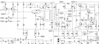
I think you should remove R77 in the diagram above and check and, as said before, pay attention to the current draw.
- Home
- General Interest
- Car Audio
- Audison LRX 4.300 "safe" mode