Follow all the VBoost path feeding the buffers - how do you supply buffers with a 68K resistor on the collector?Hi,
I have created an amp based on IRS2452 which is design-wise very similar to IRS2092 (has differential inputs).
It is based on IRAUDAMP23 (schematics attached). The MOSFETs in schematics have been replaced by IPP530N15N3GXKSA1 which have much lower Gate capacitance.
I have a problem with shoot-through when the high-side MOSFET turns off (and low-side MOSFET turns on).
Although I have gate buffers installed, the driver inside the IRS first seems to slowly discharge to VBoost and then discharges the gate(or the gate buffer transistors) faster. Due to this slow discharge, I get a shoot-through.
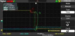
See attached photos taken between R1409 and R1408(yellow) and R1419 and R1424(blue).
Any idea what could be the root cause ?
VBoost is 45V, -VBoost -45V - the other voltages are okay as well (the amp plays well but idle current is too high).
Regards,
Beetlebuster
Hi Reactance!
While I'm experimenting on low supply voltages and connected VBoost +32V/-32V.
IRS2452AM is used as the driver.
DeadTime is set to the maximum value (105ns).
Load resistor 4 ohms, inductor 0.22uH, capacitor 0.47uF
The initial Cboot power supply is carried out through a 22K resistor to the buffer collector.
The problem is that at idle and under load, when the LO MOSFET is turned on for a long time, the HI MOSFET opens too early and closes too late.
In all other cases, the pulses are almost perfect.
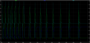
I made an imitation in the LTspice program and I got the results of the waveforms exactly the same as on the really assembled circuit, so I will give the circuit and the waveforms from LTspice.
The diagram in the red rectangle exactly corresponds to the real one. Except that the power supply is unipolar 24 volts. The main thing is that the problem can be traced.
DeadTime in LTspice 140ns - as practice has shown, changing DeadTime does not affect this problem.
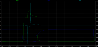
The waveform shows that when the LO MOSFET is turned on for a long time and the HI MOSFET is turned on briefly immediately after the LO MOSFET is turned off (without DeadTime), a voltage appears on the HI MOSFET gate that falsely turns on the HI MOSFET.
This voltage drops immediately after the LO MOSFET is turned on.
The diagram of the current taken from the resistor R21 shows that the pulses from the driver come correctly, taking into account the DeadTime.
It looks like this is some kind of voltage associated with the parasitic capacitances of the transistor.
While I'm experimenting on low supply voltages and connected VBoost +32V/-32V.
IRS2452AM is used as the driver.
DeadTime is set to the maximum value (105ns).
Load resistor 4 ohms, inductor 0.22uH, capacitor 0.47uF
The initial Cboot power supply is carried out through a 22K resistor to the buffer collector.
The problem is that at idle and under load, when the LO MOSFET is turned on for a long time, the HI MOSFET opens too early and closes too late.
In all other cases, the pulses are almost perfect.
I made an imitation in the LTspice program and I got the results of the waveforms exactly the same as on the really assembled circuit, so I will give the circuit and the waveforms from LTspice.
The diagram in the red rectangle exactly corresponds to the real one. Except that the power supply is unipolar 24 volts. The main thing is that the problem can be traced.
DeadTime in LTspice 140ns - as practice has shown, changing DeadTime does not affect this problem.
The waveform shows that when the LO MOSFET is turned on for a long time and the HI MOSFET is turned on briefly immediately after the LO MOSFET is turned off (without DeadTime), a voltage appears on the HI MOSFET gate that falsely turns on the HI MOSFET.
This voltage drops immediately after the LO MOSFET is turned on.
The diagram of the current taken from the resistor R21 shows that the pulses from the driver come correctly, taking into account the DeadTime.
It looks like this is some kind of voltage associated with the parasitic capacitances of the transistor.
Attachments
When connecting the C17/R31 and C18/R32 snubber, the HI MOSFET is turned on correctly, the shutdown also occurs with a delay.
In any case, this cannot be a solution to the problem, since a very large current flows through such a snubber, a very powerful resistor and a large film capacitor are needed. I haven't tried this option on a real circuit.
Reducing the capacitance of the capacitor in the snubber does not solve the problem of early activation of the HI MOSFET.
Attachments

Hi alexey496
If I understand you correctly, you are looking at the behavior at clipping, that is where the duty cycle of the pulses becomes close to 1 and 0. Correct.
This will always trigger some more complex switching behavior.
I think you first need to secure that the "normal" switching is working well.
What is the exact circuit you have built, please post, otherwise it's a bit difficult to help 😉
IPP530 does not need the extra discrete drivers, so you could try omitting these to simplify.
You of course need a stable 12 V (14V is even better) supply for the drivers.
The Cboot (C9 in your TSpice) is larger than really needed, and you should try a smaller value to start with to ensure proper startup. 1uf X7R is enough.
The resistor from the rail+ to Cboot, need to be small enough to charge Cboot at startup, which depends on the rail+ voltage. For +30Vdc use 15k.
IPP530 is an Optimos3 mosfet, which is not that easy to work with. It is very similar to the IPP320N20N3 which I have tried out, and have found not really ideal (search for my post on this). To start with maybe use something which is easy to get to work well without special attention, snubbers etc. e.g. IRFB5620, IRFB4020 or even IRF640N
When using the extra drivers, you can also lower the gate resistor to 10 ohm or less, to get steeper switching edges
Last edited:
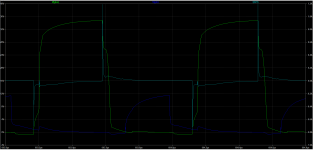
All right. Normal switching works almost perfectly, as in textbooks (see image waveform_normal in post 22).
I use a linear stabilizer to stabilize the 12V.
The real scheme corresponds to the image in post 22. Diagram circled in red fully corresponds to the actually assembled scheme.
I use IRFB5620 transistors with a buffer as shown in the diagram. I also tried to connect the IRFB4020 without using a buffer with Rg 18 ohms.
I tried disabling the diode to discharge the gate MOSFET. I tried to change the buffer transistors. I removed resistor between the base and emitter in the buffer.
In all cases, this effect remains. I don't know what else to try to fix it anymore.
I will take your advice and try to reduce the Cboot and the Cboot charging resistor. Thanks.
I'm still not sure what you problem you are facing? ... sorry
Could you either post here or send me PM the sim file? Then I'll take a look.
Also again it would be helpful to see pictures of the implementation and also see the actual schematics ..
- You say you have shoot through ... this will heat the fets right away ... is this what you see?
- Heat can as explained earlier, also com from a non ideal coil ... I have had many troubles with coils like 1D17A-220
- We would like to see a "digital" voltage signal on the gate driver output .... but as this is connected to the gate and other components, it will not behave like like that, it will be more complex. Look at the Ciss, Croo curves ... these wary over voltage, and thereby the current will also vary .... So I still would not expect the voltage you either simulate or meassure to be "textbook"
Could you either post here or send me PM the sim file? Then I'll take a look.
Also again it would be helpful to see pictures of the implementation and also see the actual schematics ..
By the way:
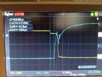
What you see in your measurement is that the first step A is the gate driver turning off (notice the step is 12V as is the driver voltage), and actually doing this really fast and text book like, then there is a delay caused by the mosfet and what ever driving circuit is in between ....
B is the voltage the gate follows, which is not the same as current running through the fet in the same way
I think what is more surprising is that you can actually see such a nice step and not a slope ...
Where is A measured ... output of the driver IC or the gate?
Attachments
The problem is heating the MOSFETs. I connected a load of 4 ohms, I supply about 5 watts of power. After 30 seconds of operation, the MOSFETs heat up so that it is impossible to hold my hand. Although maybe this is normal? since I haven't installed the radiator yet. If you do not supply an input signal with a connected load, the transistors are barely warm.
I understand that a perfect digital signal will not work. But it seems to me that shoot through is not the norm.
Although maybe I'm wrong and this behavior is the norm... I have no experience building D-class amplifiers.
I am also skeptical about SIM, I made a simulation with the hope that it will help me solve this problem.
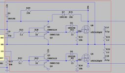
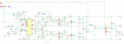
My diagram is quite large, so I give only part of it, but the most important
I understand that a perfect digital signal will not work. But it seems to me that shoot through is not the norm.
Although maybe I'm wrong and this behavior is the norm... I have no experience building D-class amplifiers.
I am also skeptical about SIM, I made a simulation with the hope that it will help me solve this problem.
My diagram is quite large, so I give only part of it, but the most important
Attachments

You using an IN4148 to supply your drive circuit ? It's rated at 500mA peak, 150mA average. what ever is happening at the drive effects the switching output, fix/clean and trace around the supply nodes. How did you arrive at this schematic ?Hi Reactance!
While I'm experimenting on low supply voltages and connected VBoost +32V/-32V.
IRS2452AM is used as the driver.
DeadTime is set to the maximum value (105ns).
Load resistor 4 ohms, inductor 0.22uH, capacitor 0.47uF
The initial Cboot power supply is carried out through a 22K resistor to the buffer collector.
The problem is that at idle and under load, when the LO MOSFET is turned on for a long time, the HI MOSFET opens too early and closes too late.
In all other cases, the pulses are almost perfect.
I made an imitation in the LTspice program and I got the results of the waveforms exactly the same as on the really assembled circuit, so I will give the circuit and the waveforms from LTspice.
The diagram in the red rectangle exactly corresponds to the real one. Except that the power supply is unipolar 24 volts. The main thing is that the problem can be traced.
DeadTime in LTspice 140ns - as practice has shown, changing DeadTime does not affect this problem.
The waveform shows that when the LO MOSFET is turned on for a long time and the HI MOSFET is turned on briefly immediately after the LO MOSFET is turned off (without DeadTime), a voltage appears on the HI MOSFET gate that falsely turns on the HI MOSFET.
This voltage drops immediately after the LO MOSFET is turned on.
The diagram of the current taken from the resistor R21 shows that the pulses from the driver come correctly, taking into account the DeadTime.
It looks like this is some kind of voltage associated with the parasitic capacitances of the transistor.
this is a complete copy IRAUDAMP23:
https://www.infineon.com/dgdl/Infin...N.pdf?fileId=5546d462677d0f4601679746020259b4
1N4148 is also used there.
Do you think the current of these diodes will not be enough? I remove them out after the tests and checked - they are fine...
https://www.infineon.com/dgdl/Infin...N.pdf?fileId=5546d462677d0f4601679746020259b4
1N4148 is also used there.
Do you think the current of these diodes will not be enough? I remove them out after the tests and checked - they are fine...
Barlin, I tried to reduce the Cboot and the Cboot charging resistor, but it didn't fix the problemHi alexey496
If I understand you correctly, you are looking at the behavior at clipping, that is where the duty cycle of the pulses becomes close to 1 and 0. Correct.
This will always trigger some more complex switching behavior.
I think you first need to secure that the "normal" switching is working well.
What is the exact circuit you have built, please post, otherwise it's a bit difficult to help 😉
IPP530 does not need the extra discrete drivers, so you could try omitting these to simplify.
You of course need a stable 12 V (14V is even better) supply for the drivers.
The Cboot (C9 in your TSpice) is larger than really needed, and you should try a smaller value to start with to ensure proper startup. 1uf X7R is enough.
The resistor from the rail+ to Cboot, need to be small enough to charge Cboot at startup, which depends on the rail+ voltage. For +30Vdc use 15k.
IPP530 is an Optimos3 mosfet, which is not that easy to work with. It is very similar to the IPP320N20N3 which I have tried out, and have found not really ideal (search for my post on this). To start with maybe use something which is easy to get to work well without special attention, snubbers etc. e.g. IRFB5620, IRFB4020 or even IRF640N
When using the extra drivers, you can also lower the gate resistor to 10 ohm or less, to get steeper switching edges
It looks like you are actually using ES1D diodes for the power lines, and not 1N4148 ... should be good ... also what I use.
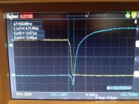
What are the exact conditions in the picture in post #31 ?
I do not like the look of the blue coil ... but being gapped it can probably work. Is the other a T106-2? ....
If you are drawing 5W continuously the fets will start to heat .... .... if everything stays cool witout signal, I think you are on the right track.
Frequency is 363 kHz as read on the scope? .... also a good sw freq
I do not know which diode you mean. In parallel with Rg, I use exactly 1N4148 as in the original IRAUDAMP23 scheme. The rest are ES1G (a higher voltage version of ES1D).It looks like you are actually using ES1D diodes for the power lines, and not 1N4148 ... should be good ... also what I use.
What are the exact conditions in the picture in post #31 ?
I do not like the look of the blue coil ... but being gapped it can probably work. Is the other a T106-2? ....
If you are drawing 5W continuously the fets will start to heat .... .... if everything stays cool witout signal, I think you are on the right track.
Frequency is 363 kHz as read on the scope? .... also a good sw freq
Measurement conditions in post 31: idle frequency 338 kHz, voltage +32/-32V, load 4 ohms, power 5 W, DT 65 ns.
I have two types of coils T106-2, as you correctly noticed, and ferrite with a gap of more than 2 mm. This is necessary for experiments.
The frequency with connected load and shorted inputs is 338 kHz.
I do not know which diode you mean. In parallel with Rg, I use exactly 1N4148 as in the original IRAUDAMP23 scheme. The rest are ES1G (a higher voltage version of ES1D).
Measurement conditions in post 31: idle frequency 338 kHz, voltage +32/-32V, load 4 ohms, power 5 W, DT 65 ns.
I have two types of coils T106-2, as you correctly noticed, and ferrite with a gap of more than 2 mm. This is necessary for experiments.
The frequency with connected load and shorted inputs is 338 kHz.
C36 and C37 please review this capacitors I'm not happy with the fact that the bootstrap cap has to charge that up as well during its discharge cycle also what type of capacitors are you using for bootstrap hopefully tantalum and the polarity is correct.The problem is heating the MOSFETs. I connected a load of 4 ohms, I supply about 5 watts of power. After 30 seconds of operation, the MOSFETs heat up so that it is impossible to hold my hand. Although maybe this is normal? since I haven't installed the radiator yet. If you do not supply an input signal with a connected load, the transistors are barely warm.
I understand that a perfect digital signal will not work. But it seems to me that shoot through is not the norm.
Although maybe I'm wrong and this behavior is the norm... I have no experience building D-class amplifiers.
I am also skeptical about SIM, I made a simulation with the hope that it will help me solve this problem.
My diagram is quite large, so I give only part of it, but the most important
After looking at your TSpice sim output, I for sure think it looks wrong ....
Again, if you could send me the sim files, I could give it a go .... there must be something wrong ..
Which model are you using for the IRS driver?
Again, if you could send me the sim files, I could give it a go .... there must be something wrong ..
Which model are you using for the IRS driver?
- Home
- Amplifiers
- Class D
- Dead-Time issue with IRS2092/2452AM