Hi juma,
That link is for current drive of the power transistors almost the same as used this thread.
The improvement I was thinking that keantoken did was for the topology in Electronics World Wim De Jager article Dec 1999 cited in Post 23 by Mooly. PM him, he may remember it. It's not directly relevant to the topology in this thread.
Hi Kay,If that horizontal 8 ohms resistor between inv and Out marked RL is really the load, this design shows current feedback (NFB signal proportional to the output current), rersulting in a very high output impedance. Is this intended?
Best regards!
Yes, it is intended. It gives current feedback in the traditional canonical sense.
I think I am correct in saying that it is not CFA. But I don't really want to debate the CFA vs VFA thing here.
I'd prefer to keep this thread to the advantages/disadvantages of the topology (eg see Post 2).
I find it has a lot of advantages over my last posts on the wideband autobias I tested, eg Post 157 here https://www.diyaudio.com/community/...ching-auto-bias-power-amp.375141/post-7039868
When you add more feedback to this output stage you can either use voltage feedback or current sense feedback signal.
If you use voltage feedback then just an extra 20dB can make the output resistance of the amplifier low enough to drive almost any loudspeaker.
If you use more current sensed feedback then you need custom loudspeakers with equalization for the changed frequency response of the drivers and a different passive crossover network.
Hi Damir,Hi Ian,
Ok my bad. I have that Electronics World (and many others) and keep it on separate place where I have it to read it carefully again. It was long time ago with no spice available and not easy to test all kind of feedback.
Now I will reread it again, thanks Ian.
I have Orion speakers with active analogue crossovers(Linkwitz) before output power amps.
Do you think about using transconductance amps instead voltage drive amps (CFA) I am using now, do I need to change something in the existing crossovers?
BR Damir
Sorry to delay. Since you have an active crossover it is easier to change to current drive (transconductance amps).Do you think about using transconductance amps instead voltage drive amps (CFA) I am using now, do I need to change something in the existing crossovers?
You have the choice of changing the mid and high amps to current and leaving the low with voltage. I'm hoping that may give almost the same overall response and if not the active crossovers could be altered slightly, but I haven't tried this approach and it depends on your particular drivers and crossovers.
If you change the low to current then you need to add an equalizer to suppress the resonance. There are various equalizers, the Linkwitz transform is a fixed frequency fixed Q design. I have only used a tuneable fo and independently tuneable Q equalizer that I modified from an Electronics World Article by Sokol, 'Practical-Subwoofer-Design', Wireless World Dec 1983, p41 (https://worldradiohistory.com/UK/Wireless-World/80s/Wireless-World-1983-12.pdf) I found it easy to tune out the bass resonance by ear. Since then I realised it is easier/quicker to use pink noise (which I didn't have until recently) and the resonance then stands out in the pink noise as a definite tone! that you then remove manually with the equalizer. Another independently tuneable equalizer is given in Esa's book (linked Post 29).
Unfortunately, I can't find anyone posting on this forum who have used these simple analog based equalizers to convert to current drive. I found one post using DSP by Jerry R here https://www.diyaudio.com/forums/sol...rrent-drive-voltage-drive-lf-post5211708.html.
OldDIY, do you have links to some more recent (modern) builds of Dorofeev's amp from Russian forums?#7, #12 http://archive.radio.ru/web/1991/03/056/
Dorofeev's amplifier, which is very popular with Russian DIY.
I guess logically, it changes a fair amount with signal, ~15%. For 1Vin peak, at signal peaks G(inv) increases as Q3 and Q4 re decreases with increased emitter current, and AC analysis is only working with small signal at DC op pt, and closed loop transconductance follows. At 100mVin G(inv) and transconductance gain are more stable, with ~1.3% change in transconductance gain from peak to trough. My numbers could be a little off since I just tried to measure trough value to the point before the 0 crossing spike artifact (maybe there's a way to avoid dividing by 0?)Based on post 29, i think he does intend current drive. Transconductance is consistent across speaker load with .22R current sense. Transconductance is (Gain at inverting node)/RSense, i.e. V(Inv)/V(in)/Rsense, at least for 8 ohm load and RS between .11 and 1R. Thats as far as I got so far, all in AC. Not sure how easy or worthwhile it is to increase Gain at inverting node, or how much it changes with signal.
Attachments
Hi dkfan9,
To get A/V you first use two cursors on I(RL) slightly different times and read off the slope at the bottom of the cursor box. You then use a calculator to divide the derivative reading by the slope value. This is the scaling factor to convert d(I(RL)) reading to A/V.
To plot Gm plot d(I(RL)). But it is the derivative wrt to time.(maybe there's a way to avoid dividing by 0?)
To get A/V you first use two cursors on I(RL) slightly different times and read off the slope at the bottom of the cursor box. You then use a calculator to divide the derivative reading by the slope value. This is the scaling factor to convert d(I(RL)) reading to A/V.

Hi All,
I was browsing Esa Mirilainen's site and found the Articles Elsewhere page https://www.current-drive.info/seealso/73. At the bottom is a link to a loudspeaker manufacturer making an active unit using using current drive https://www.stereonet.com/au/news/sgr-audio-releases-world-first and says
I was browsing Esa Mirilainen's site and found the Articles Elsewhere page https://www.current-drive.info/seealso/73. At the bottom is a link to a loudspeaker manufacturer making an active unit using using current drive https://www.stereonet.com/au/news/sgr-audio-releases-world-first and says
It is dated late 2016. BTW Has anyone here listened to these speakers or own a pair?This new technology is said to provide a sonic difference that is astoundingly clear and amazing. At the time of writing, it's believed that SGR Audio are the first in the world to implement current-drive technology in a commercially available loudspeaker.
Hmm... I think I might be misunderstanding. When I use this technique [value for d(i(rl))/slope of i(rl) at points close to where d(i(rl)) is measured], I get values very close to 1, which is obviously not correct for Gm... The d(i(rl))/d(v(in)) plot looks useful though it still has spikes (this time at signal peaks, but not to infinity).Hi dkfan9,
To plot Gm plot d(I(RL)). But it is the derivative wrt to time.
To get A/V you first use two cursors on I(RL) slightly different times and read off the slope at the bottom of the cursor box. You then use a calculator to divide the derivative reading by the slope value. This is the scaling factor to convert d(I(RL)) reading to A/V.
I've been playing around with the circuit, I found reduced beta in the output transistors with increased bias current in the input current mirror to maintain identical output bias current results in lower distortion. With 1Vin, At BF=50, THD=1.42%, at BF=158, THD=1.59%. The practical downsides I saw were increased current draw in those transistors at high signal levels and higher DC offset, but I thought it might be a useful piece of information. Most of the other things I tried did nothing (e.g. different zener reference point) or caused oscillation (CFP around Q3/4). Increasing RS decreases distortion and reduces Gm in proportion with value change [scaling input voltage to account for Gm change].
As for current drive speakers, another one on the block is the Kii Three, but I haven't heard them.
the derivative is the same thing as the slope so you're dividing it by itself and the result is 1.When I use this technique [value for d(i(rl))/slope of i(rl) at points close to where d(i(rl)) is measured], I get values very close to 1
gm is dI/dV, with I=output current, and V=voltage between the input and the output of whatever you want to measure gm of, for example the output stage.
Note if the load is a resistor R, dVout/dIout is always equal to R. gm is not about Vout, it is about the current dependent voltage drop across the output stage...
Hi dkfan9,
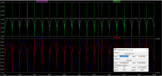
Sorry, my bad 😳 . The scale factor is not from the slope of I(RL) but slope of V(in).
For Gm I use a triangle wave so the slope of V(in) is a constant including the zero crossing. I use freq=1 for Gm plots and got the slope of V(in) =1.2V/s as screen shot:
-V(in).png")
I realised after my post was that you can enter the units in the plot equation to read out as A/V (actually says Ohms^-1 which is the same).
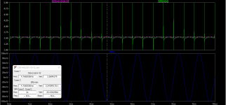
So the revised method is enter d(I(Rl))/1.2V*1s as the plot as screen shot:
)over1.2Vtimes1s.png")
Note: If you change freq then you need to enter a new scale value for the slope of V(in).
And for the THD and FFT I change to a sinewave and usually change to 1kHz and set the Vpk level for the power you want.
Alternatively, using the calculator method and d(I(RL)) I get 17.83A/s ( screen shot). Divide that by 1.2V/s gives Gm of 14.86A/V (same as above).
).png")
Sorry, my bad 😳 . The scale factor is not from the slope of I(RL) but slope of V(in).
For Gm I use a triangle wave so the slope of V(in) is a constant including the zero crossing. I use freq=1 for Gm plots and got the slope of V(in) =1.2V/s as screen shot:
I realised after my post was that you can enter the units in the plot equation to read out as A/V (actually says Ohms^-1 which is the same).
So the revised method is enter d(I(Rl))/1.2V*1s as the plot as screen shot:
Note: If you change freq then you need to enter a new scale value for the slope of V(in).
And for the THD and FFT I change to a sinewave and usually change to 1kHz and set the Vpk level for the power you want.
Alternatively, using the calculator method and d(I(RL)) I get 17.83A/s ( screen shot). Divide that by 1.2V/s gives Gm of 14.86A/V (same as above).
Hi All, A comparison of 1) cross-base charge pull-out, and 2) Miller neutralization, and 3) none of these.
The current drive of the power transistors in this thread (CSD) requires that no base-emitter resistors be used for the power transistors. These resistors are used in normal power stages such as the CFP to speed up the charge removal from the power transistors to turn them off faster, to reduce cross-conduction at high frequencies. Without them cross conduction becomes a serious issue at 20kHz so some alternative form of charge removal is needed for CSD output stages.
1) The simple alternative, as used in the Dorofeev amps (Post 44), with a capacitor (100nF) and series resistor (200R-1k) couples the bases of the power transistors is quite effective allowing safe operation at 20kHz and above.
2) Miller neutralization (Post 2) uses an inverting opamp with a voltage gain of -0.1 drives two C+R networks (1nF-3nF and 100-300R). The opamps prevents supply rail noise getting into the bases due to the opamps low output resistance. Also the two C+R networks can be trimmed to optimise for different capacitances of the PNP and NPN power transistors.
First a look at no charge pull-out for my circuit at 20kHz (Post 2 with Cc=0) Circuit 3 in the attached files:

Notice the crossover kink in V(out). There is a slow turn off of collector currents (tail) and a delayed turn on at the zero-crossing. The idle current at 1kHz is 210mA each but at 20kHz one increases and the other falls.
Now with the C+R of 100nF + 22 ohms (Circuit 4) at 20kHz:

The kink at crossover is removed and the tail currents are corrected and the crossover currents are about the same (but only when the series R is in the 10-22 ohm range!). The idle current has increased from 210mA to 375mA so cross-conduction is still a concern with this charge-pull out method.
For Miller neutralization (100R+3nF for PNP and 1n5 +100R for NPN) at 20kHz (Post 2 circuit):

This gives less increase in idle current at 20kHz and the currents track with increasing frequency better (thanks to half the base capacitance for the NPN than the PNP).
A further modification allows the power transistor currents to stay above 20mA when the other transistor current peaks for the "non-switching" mode. It is a "keep-on" resistor between the two power transistor bases for about 200uA (470k with 45V rails). It stops the FT of the power transistors falling so they can turn-on faster.

BTW if you add this resistor across the other C+R inter-base network then at 20kHz and above one transistor stays on but the other doesn't (presumably because the PNP and NPN capacitances are different). If you raise the keep on current further so both stay on you have too much added idle current at idle and for the lower frequencies.
-----------------------
Conclusion: Miller neutralisation allows safe operation at 20kHz and above. It also allows independent balancing of the PNP and NPN capacitance differences which then permits some useful (20mA) keep-on current in the power transistors.
Apart from removing cross-conduction at 20kHz you get almost the same harmonic structure at 20kHz as at 1kHz.
I think this gives the CSD output stages about the same high frequency top end as standard Darlington and CFP output stages but with less thermal issues and a better harmonic structure.
The current drive of the power transistors in this thread (CSD) requires that no base-emitter resistors be used for the power transistors. These resistors are used in normal power stages such as the CFP to speed up the charge removal from the power transistors to turn them off faster, to reduce cross-conduction at high frequencies. Without them cross conduction becomes a serious issue at 20kHz so some alternative form of charge removal is needed for CSD output stages.
1) The simple alternative, as used in the Dorofeev amps (Post 44), with a capacitor (100nF) and series resistor (200R-1k) couples the bases of the power transistors is quite effective allowing safe operation at 20kHz and above.
2) Miller neutralization (Post 2) uses an inverting opamp with a voltage gain of -0.1 drives two C+R networks (1nF-3nF and 100-300R). The opamps prevents supply rail noise getting into the bases due to the opamps low output resistance. Also the two C+R networks can be trimmed to optimise for different capacitances of the PNP and NPN power transistors.
First a look at no charge pull-out for my circuit at 20kHz (Post 2 with Cc=0) Circuit 3 in the attached files:
Notice the crossover kink in V(out). There is a slow turn off of collector currents (tail) and a delayed turn on at the zero-crossing. The idle current at 1kHz is 210mA each but at 20kHz one increases and the other falls.
Now with the C+R of 100nF + 22 ohms (Circuit 4) at 20kHz:
The kink at crossover is removed and the tail currents are corrected and the crossover currents are about the same (but only when the series R is in the 10-22 ohm range!). The idle current has increased from 210mA to 375mA so cross-conduction is still a concern with this charge-pull out method.
For Miller neutralization (100R+3nF for PNP and 1n5 +100R for NPN) at 20kHz (Post 2 circuit):
This gives less increase in idle current at 20kHz and the currents track with increasing frequency better (thanks to half the base capacitance for the NPN than the PNP).
A further modification allows the power transistor currents to stay above 20mA when the other transistor current peaks for the "non-switching" mode. It is a "keep-on" resistor between the two power transistor bases for about 200uA (470k with 45V rails). It stops the FT of the power transistors falling so they can turn-on faster.
BTW if you add this resistor across the other C+R inter-base network then at 20kHz and above one transistor stays on but the other doesn't (presumably because the PNP and NPN capacitances are different). If you raise the keep on current further so both stay on you have too much added idle current at idle and for the lower frequencies.
-----------------------
Conclusion: Miller neutralisation allows safe operation at 20kHz and above. It also allows independent balancing of the PNP and NPN capacitance differences which then permits some useful (20mA) keep-on current in the power transistors.
Apart from removing cross-conduction at 20kHz you get almost the same harmonic structure at 20kHz as at 1kHz.
I think this gives the CSD output stages about the same high frequency top end as standard Darlington and CFP output stages but with less thermal issues and a better harmonic structure.
Attachments
Thanks for the calculus refresher, it's been a while 😀the derivative is the same thing as the slope so you're dividing it by itself and the result is 1.
gm is dI/dV, with I=output current, and V=voltage between the input and the output of whatever you want to measure gm of, for example the output stage.
Note if the load is a resistor R, dVout/dIout is always equal to R. gm is not about Vout, it is about the current dependent voltage drop across the output stage...
Yes, that's what I was thinking above, dIout/dVin. I'll have to try it with the triangle wave Ian mentions.
What about the two Akai emitterless units? The AM-U5 and the AM-U7.
I have a U7 sitting here, and could buy a minty U5 by this afternoon. I know of a local store that has one and no one knows how 'special' or rare it is. I bought the AM-U7 to have a known 'reliable' emitterless design around, in case I wanted to do some experiments in improving the circuit. I have my ideas....the same tricks I used to get 4-6-8 transistor per rail AB amplifiers to sound like single transistors per rail designs.
My test units for the innovation were a RAMSA WP-9440, a weird design if there ever was one, and a USA850. both sound hugely better than their original circuit did. the USA850 is loads better than stock. Audiophile even. which is a vast improvement over stock, as they are pretty well unlistenable, in my book, in stock form. a USA 850 with punch, finesse, depth, speed, detail, shimmer, liquidity, plosives, and the rest? How strange would that be? My point being, is that the circuit innovation involved would really show itself with emitterless designs.
In this case, with the AM-U7, it is a 80-90 wpc rated version of such emitterless thinking. Hifi-engine only has the schematic for the AM-U5. the U7 appears to be the same with a punched up rail voltage. they both have no real rated power into 4 ohms, on paper (stated specs), so this seems to speak to some of the issues raised in this thread, but I've only read the first few posts. I then checked to see if the AKAI units were mentioned in the thead (approx 1984 build/design dates), and they were not. thus, the reasoning behind this post.
Last edited:
You are right, I just checked by opening up my U7, as I had this niggling remembrance of seeing emitters..
Their 'trick' as it were, is zero feedback in the output stage. I had forgotten what exactly the trick was, that they had.
my bad. Wrong Pew!
Almost as if there are two camps for going commando in the quest for solid state liquidity in sound quality. No emitters, or zero feedback. And I forgot which shorts or lack thereof, that I was dealing with today.
I might as well add something that can be dismissed or talked about or has been talked about already. that, in my humble experience, in my hearing, etc..., the idea of high correction or fast correction, or attempts at dealing with overcurrent and runaway in the outputs, via pre-stage manipulation, or feedback circuits, in the idea of application to emitterless designs, sounds just as bad as high feedback circuits, if not worse. i am not fond of any of the high feedback class B or class AB designs out there (BJT, mosfet, etc). For serious listening and enjoyment...they all sound intolerable to me, now. (my caveat, re opinions etc, as found in my listening tastes and sensitivities for certain distortions inherent in such design methods.)
Last edited:
- Home
- Amplifiers
- Solid State
- Class-AB with no emitter resistors and good thermal stability and good sound