You forgot from another forum that I'm putting a resistor on the USB gnd and ferrite choke.Noise from motherboard transferring via ground plane into the USB interface too...
But if you have a special PCI USB card like me - you don't need that either.
This has a battery on + and -
Last edited:
Hi 🙂
Yes again thermometer coding. But from the note it is first 4 MSB. N=4 (2**N)-1=15.
So AD1865 has first 15 MSB "DSD" and 18-4=14 LSB R2R. Almost half of the MSBs are from segmented part.
.
Since AD1862 from internal structure have 3 MSB N=3, (2**N)-1=7 encoded to Thermometer code.
AD1862 have frst 7 MSB "DSD", and 20-3=17 LSB are R2R.
.
For first 5 MSB binary - 31 MSB thermomether... To havy and complicated to implement
Imagine how long will be segment form all 16 bits encoded from binary to thermomether.
(2**16)-1=65535 bits word...
There have been reports and not very positive Look, here, but I believe he has written more about it This oneHello.
I am wondering if anyone tried jlsound oscillator board.
I have thought of using one of Andrea M.'s clocks, or using his FIFO instead.

First 3 bits are "divided" into 7 parts of thermometer code - this does not touch the rest 17 bits ... anyway thermometer DACs are very good but almost impossible for more than 12-bits (very complicated) - that is where the R-2R technique can continue. AD1862 is 3 MSBs as thermometer + 17 LSBs as R-2R 🙂Actually that is explanation that AD1862 is NOT pure R2R dac.
But segmented DAC or hybrid DAC.
Because first 3 bits are transformed as 7 bits of Thermometer code. And going to conversion same as DSD.
Other low significant bits are classic R2R dac...
So most of the sound comes grom generated first 7 bits 🙁
As other AD and PCM dacs...
Hi Miro
please take a look in I2S Philips specification PDF.
Note WSP and WSD signals. They are essential for managing almost any digital bus.
In PDF given only WSP signal graphically. emulate WSD.
That can be of use to create WCKO (LE), and other events.
The circuits are not complicated to achieve.
.
For these dacs I would not insist on pure Right Justified (like PCM1794 dictate as must) because these earler dacs are not specified as Right Justified.
Maybe try to stick with Pacific Microsonics approach but in NOS mode?
Maybe it is easy to sheck with recent shifter. Just not shift so deep but only 1 bit from I2S MSB all words for L/R?
.
We actualy dont know are the outputs of the XMOS are clean? Maybe just for the scope eye pattern on the scope? (But even then looking like have bigger peaks at the corners of the squares - signal integrity)
But from the point of jitter and eye pattern in time we don't, and that is the only criteria for clean?
.
BTW
From my measurements most of the XMOS based interfaces has inverted MCK. (That is not happier for re-clocking and other purposes of MCK.
Amanero have right edged MCK for the example.
This is interesting technique, but I am not sure if it is possible to create it "simple" from digital ICs. It looks like job for CPLD 🤔
The first MSB is very important and must be shifted in the correct place in DAC 😉
XMOS is fast and very good but important is how the clocks are implemented. I like the implementation of this clock: http://pavouk.org/hw/audiosystem20/at32uc3a3256usbi2s.html ... (digital isolator should be omitted to achieve very low jitter).
Perfect, I'm curious about the result 🤩
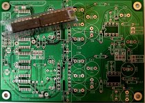
Today - is lucky day! I got new board and chips. Can't wait to assemble already! Also ordered PSU-1 for him.
Here comes the next warrior 🤩
I have been (very) slowly populating the small PSUs that @Traktorist3d shared a while back. Small dual rail PCB that are about 50x35mm at a guess just now so quite small. I'm not sure of the topology even if it is a shunt or not ...I think it's more a nazar type. Haven't tested yet but should perform wellWith all the power supply discussions recently, seems like a perfect time to ask opinions about what types of psu would be favored to include onboard an AD1862 dac.
@miro1360 Can I use electrolyte for PSU on 16V? (I need 5V on this time). I could't find nichicon 4700 and 6800 but instead Panasonic FC or Epcos.
Also I planning to solder np0 smd (GRM31C5C1H104JA01L) instead Wima on Dac board (1702) and instead Kemet (6pcs). This is for sample (I can get it back always).
Also I planning to solder np0 smd (GRM31C5C1H104JA01L) instead Wima on Dac board (1702) and instead Kemet (6pcs). This is for sample (I can get it back always).
Yes but no one said that other last significant bits are corrupted? Just want to point out the facts based on the data.First 3 bits are "divided" into 7 parts of thermometer code - this does not touch the rest 17 bits ... anyway thermometer DACs are very good but almost impossible for more than 12-bits (very complicated) - that is where the R-2R technique can continue. AD1862 is 3 MSBs as thermometer + 17 LSBs as R-2R 🙂
So the point is that AD1865 have more precise first 3 MSBs than AD1862 that have only 3 MSBs.
And there are NO R2R components like resistors. Current sources or some other active modules emulating R inside. R, C component are complicated to implement in IC...
this is science fiction to accomplish 12Bit Binary to thermometer code
it deserves (2**12)-1=4095 taps to go to R network and analog out "resistors" and very complex circuit. 🙁
For instanse we dont have any "chip" with 4095 pins and more if we want to get out with some ladder?
That is why manufacturers chose smaller number for thermometer segment.
.
True R2R ladder net, with pasive resistors, we can find just in discrete dac modules 🙁
.
For instance TDA1540 and TDA1541 are in BJT technologies, most other are witn MOSFET or mixed thech. Contemporary models are almost all with MOSFET tech. That is also can determine the sound?
.
Does not matter at the end everyone can choose by the listening what to use in reproduction 🙁
I use the oscillator board together with a gen 1 Xmos board in one of my dacs. With good clocks it provides obvious improvements upon the Xmos board, much as can be expected. The reclocking device remains the d-type on the Xmos board and the oscillator board provides merely a better regulator for the clocks and clock switching. If you have the current V3 Xmos, reclocking will still be provided by the fpga.Hello.
I am wondering if anyone tried jlsound oscillator board.
@sworder84
Raw DC voltage is important. For 16VDC filter capacitors, take 9VAC secondary transformers. For 5VDC at the output this is more than enough and the raw DC will not be over 14V at the first capacitor in the CRC. The AC voltage to the secondary is given for full load, if the transformer is less loaded that voltage rises above the rated. In any case, I recommend 25VAC filter capacitors for the first capacitor that is the most loaded. Check the spacing of the terminals on the capacitors to fit with the PCB.
The scheme published in post # 4,190 is wrong, the corrected scheme is attached. One transformer with two 12VAC secondary cannot be used with all positive regulators, but one transformer with 2x12VAC secondary and one with 2x9VAC secondary. With a combination of positive and negative regulators, only one transformer can be used. And LT1117T-5.0 TO220 were used instead of LP2950ACZ-05 TO92. I don't like those little ones in the TO92 case.I am interested in how much current the DAC consumes (with AD1865), primarily the digital part with shift registers (+ 5V). At the moment it is very difficult to get adjustable version of the LT1963/3015 so I have to make an alternative power supply. For + 5V. That’s until I get LT regulators. I plan LP2950ACZ-5.0, (TO92 100mA), for +5V digital part. The analog part with OPA will be + -12V with LM2940 CT-12 regulators. OPA is Sparkos SS3601. The analog part of the AD1865 will be + -5V with LP2950ACZ-5.0 regulators. The transformer has two 12VAC secondaries, 16VA.
PS
Capacitors 4700uF 25V can be used for + -5V power supply part. I do not recommend 16V capacitors.
This is a temporary solution, but it works.
Attachments
Last edited:
Yes I had a note about this too earlier... A few posts before. It is more like Time simoultaneous format trigering conversion not like Rigt Justified.Miro, great work! I am impressed that you could again reduce the amount of ICs - but this circuit is not the one you posted half a year ago... I did test that one for you, see here.
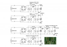
The idea of stopped clock is to have all digital lines silent when analog output updates, plus a settling time to avoid all influences caused by switching tasks inside the DAC chip. If everything is completed, the chip waits for the next event: the power rails are unburdened, it's time for update of the analog output. I tested the AD1862 by feeding pulses slowly from an MCU to it so I can watch the exact moment it updates IOUT, see attached scope shot.
So if you want to improve sound quality with stopped clock you also need to delay LE, see attached diagram! Something as shown in
Just to show how it can be done here my simulations for similar purposes:
EDIT: an LE pulse during the stopped clock would work but would slightly pollute the power rails because of the additional rising edge. Better to have the rising edge of LE during DATA transfer...
- stopped clock glue logic
- delayed LE for AD1862
- OT: solution for PCM1704
And You dont have to delay the LR latch. Just o cut out all + statec prior to the event when LE going from 1 to 0. Only that ste triggers conversion.
And It should not be imeadetly after LSB. From LSB to LE should be 3-4 BCK cycles.
There are plenty of space to put the words inside LE. With a stopped clock.
I will post some circuits...
Correct Your I2S bus. Please note that BCK of I2S is always going from 1 to 0 always when LE changed state.
So invert RCK line and repeat sim?
Which capacitors exactly?@miro1360 Can I use electrolyte for PSU on 16V? (I need 5V on this time). I could't find nichicon 4700 and 6800 but instead Panasonic FC or Epcos.
Also I planning to solder np0 smd (GRM31C5C1H104JA01L) instead Wima on Dac board (1702) and instead Kemet (6pcs). This is for sample (I can get it back always).
It is most important to understand that finishing register loading and LE changing state from 1 to 0 is happening almost instantly. And that is the cae ONLY if Rigt Justified format used... Because of that only LE in this case has to be precise but other syncs are also important. And Jitter in time can have max afect.I did 🙂 This system with flip-flops is not "re-clock" but more like "re-align" data. It is not solution for eliminating jitter - in our case the most critical signal for AD1862 - the LRCK. When the source outputs jittered LRCK, it stays jittered also after the flip-flops. If you want true reclock, then the LRCK must be generated from a new clean clock (like 44.1kHz or 48kHz) and this LRCK should synchronize the I2S data (it can be complicated).
... for generating new LRCK from a clean clock a ripple counter can be used (see the 74HC4040) https://pc.watch.impress.co.jp/docs/2004/1005/nidac_ah7.jpg
https://tinyurl.com/2zr7wcff 😎
... better as delayed LRCK can be delay other data and the LRCK left as clean as possible (for the AD1862), ... this can be job for CPLD ... what do you think?
IF you left few bits of BCK when registers are already loaded, and LE stays in place, jitter could not be from that importance and DAc have much more time to "rest" and go to the conversion.
That is Whu Time Simultaneous format did this and Pacific Microsonic done the same - left blank sertain amount of BCKs prior to LE change state.
.
Only if we have 32 bit word we simply have to use all 32 bit for channel word and make it like pure Right Jusified format.
In all other cases we dont have to.
For 24 bit word we have 4 bits at each side of the word and 4 bits before each command to conversion.
What do you mean by "bits are corrupted"?Yes but no one said that other last significant bits are corrupted? Just want to point out the facts based on the data.
So the point is that AD1865 have more precise first 3 MSBs than AD1862 that have only 3 MSBs.
And there are NO R2R components like resistors. Current sources or some other active modules emulating R inside. R, C component are complicated to implement in IC...
this is science fiction to accomplish 12Bit Binary to thermometer code
it deserves (2**12)-1=4095 taps to go to R network and analog out "resistors" and very complex circuit. 🙁
For instanse we dont have any "chip" with 4095 pins and more if we want to get out with some ladder?
That is why manufacturers chose smaller number for thermometer segment.
.
True R2R ladder net, with pasive resistors, we can find just in discrete dac modules 🙁
.
For instance TDA1540 and TDA1541 are in BJT technologies, most other are witn MOSFET or mixed thech. Contemporary models are almost all with MOSFET tech. That is also can determine the sound?
.
Does not matter at the end everyone can choose by the listening what to use in reproduction 🙁
Thermometer from MSBs in AD1862/AD1865 is not for a higher precision, but rather for eliminating glitch. R-2R ladder is inside the AD1862/5 for the LSBs, is not?
Hard to say if the full R2R ladder is incorporated in any advanced R2R chips, even DAC8811 has the 3 MSBs segmented and the rest is R2R 🤔
Exactly, the listening test is the best way 😊
- Home
- Source & Line
- Digital Line Level
- DAC AD1862: Almost THT, I2S input, NOS, R-2R