Two bits aren't quite right yet:
R13 should be 200 Ohms and is in the right place. The base of Q4 should not connect directly with the 5v rail. Instead LED3 should connect between Q3 base and the 5v rail.Q3 collector should connect directly to the junction of R9 and R10 and there should be a 3k ohm resistor between Q3 base and GND to bias the LED on. With this the collector of Q4 will deliver approx 5mA of constant current,
Also R14 should connect between 5v and pin 7 of IC2, and C9 should be connected in parallel with C8 (but it is OK if it is not as close to IC2 as C8 should be).
For what it is worth I have used this arrangement many times on Jung regs.
John
Thank you very much for your suggestions, if I have not translated badly, should it be like this? Sorry but miominglese is not that good (and neither is google translate)Two bits aren't quite right yet:
R13 should be 200 Ohms and is in the right place. The base of Q4 should not connect directly with the 5v rail. Instead LED3 should connect between Q3 base and the 5v rail.Q3 collector should connect directly to the junction of R9 and R10 and there should be a 3k ohm resistor between Q3 base and GND to bias the LED on. With this the collector of Q4 will deliver approx 5mA of constant current,
Also R14 should connect between 5v and pin 7 of IC2, and C9 should be connected in parallel with C8 (but it is OK if it is not as close to IC2 as C8 should be).
For what it is worth I have used this arrangement many times on Jung regs.
John
Attachments
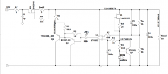
Tix88, you have these two options for CCS. I would always choose jfet, e.g. 2SK3557, CPH3910 or 2SK117 for GLED431, for simplicity and slightly better performance. I tested NSVJ6904 as a CCS today and I am pleased with the results.
Attachments

I had misread John's directions in fact the changes are wrong, thanks Grunfs for your schematics.
Try using UF4007 diodes or other soft recovery diodes and Quaismodo CRC bridge snubbing - that will help reduce rectification noise.
Hi, where can I find information?Try using UF4007 diodes or other soft recovery diodes and Quaismodo CRC bridge snubbing - that will help reduce rectification noise.
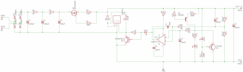
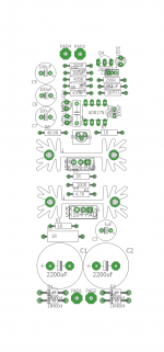
Thanks a lot, modified scheme and it should be complete. What precautions should I take for pcbs? Is there a better ground plane arrangement than someone else?View attachment 1031963
A picture paints a thousand words. This is what I was trying to describe earlier.
John
Tix88,
If it's not to much of a hassle, could you include a dual footprint for DIP8 & SOIC8 opamps?
If it's not to much of a hassle, could you include a dual footprint for DIP8 & SOIC8 opamps?
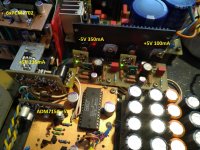
The picture shows three Walt Jung shunt regulators in my DAC, the ADM7150 remained for powering the PMD100 interface, everything else was switched to shunt regulators (before i had 2 x ADM7150 for PMD100 and +/- 5V salas shunt for PCM1702) . In the same DAC I also tried the classic Walt Jung regulators, but for digital shunt is much better and Walt shunt proved to be the best of all shunt regulators I have tried.
The TDA1541 also works better with shunt regulators, probably the same story will be for the AD1862.
The problem with shunt regulators is higher dissipation but that is a small price to pay for better sound .
The TDA1541 also works better with shunt regulators, probably the same story will be for the AD1862.
The problem with shunt regulators is higher dissipation but that is a small price to pay for better sound .
Attachments
I use 9 of Walt’s super regulators as pre-regulators for Borbely all discrete jfet/Fet shunt regulators updated to use LED voltage reference with Walt’s 2N5486 cascode of Semitec CCS. The Dac is Borbely single stage direct coupled all discrete jfet/Fet with 85 ma bias current with 8 of 1704K running at 24/192 built by Les Bordelon. I sourced the parts and built the boards. 200,000 uf power supply with CRC Quasimodo snubbed hexfet bridges. Blackgate and Teflon caps. TX 2575 resistors, 48 of 2 and 1/2inch TO220 heatsinks


Last edited:

Try the Quasimodo thread on DIYaudioHi, where can I find information?
Thanks for this thread. I had designed a PCB (all SMD) with a mashup of the GLED and walts shunt, with some of the recent additions, but had not seen many people build these yet. Will report back when I have something more final.
Hello everybody. Due to work, I was not very present and I could not carry on the project, I believe that on Sunday I will be able to share the first version of the pcb.
A question to all of you, how useful could it be to separate all transformers for each individual shunt? Would it be worth it?
A question to all of you, how useful could it be to separate all transformers for each individual shunt? Would it be worth it?
If your asking if each shunt psu output should have its own secondary winding from the power transformer, I’d say yes.
A transformer with two secondary windings could power a pair of positive output shunt psu’s 👍
A transformer with two secondary windings could power a pair of positive output shunt psu’s 👍
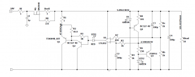
Keep the PCB as small as possible so that it can be placed as close as possible to the load itself. It is not necessary to have a rectifier on the PCB.This is the draft of the arrangement of the components, to maintain a length of 10cm.
On this version with GLED431 and jfet CCS the serial transistor has no heatsink at all, and for the input CCS only a small PCB serves as a heatsink. The voltage drop on the regulator is only 4V so BSP149 was used instead of DN2540.
Attachments
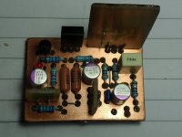
not serial transistor but SHUNT transistor 😉Keep the PCB as small as possible so that it can be placed as close as possible to the load itself. It is not necessary to have a rectifier on the PCB.
On this version with GLED431 and jfet CCS the serial transistor has no heatsink at all, and for the input CCS only a small PCB serves as a heatsink. The voltage drop on the regulator is only 4V so BSP149 was used instead of DN2540.
- Home
- Amplifiers
- Power Supplies
- Walt Jung shunt Design