Ohh White Dragon You Will Save My Lot of Time By Doing This. Thank U So Much From Heart And Soul....I will make schematic for you

I Will Definately Wait for Your Schematic..👍
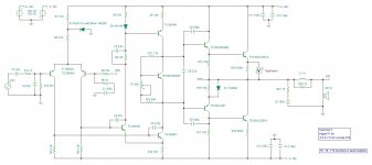
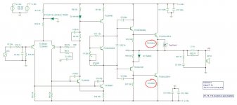
This is same amplifier with improvements
T6 , R11 and R12 is VBE Multiplier
P1 adjust bias current.
T6 is mounted on same heatsink as NPN power transistors T9 and T10
it will thermally track output transistors.
Bias Current for output transistors usually 30ma each
To adjust bias look at schematic " test point 1"
Adjust P1 for 6.5 to 7.2 mV across R19
I made values of resistors so bias is about
right with P1 centered
Still need to measure voltage drop across R19
to confirm
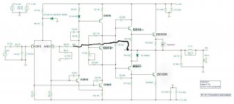
Attachments

The basic circuit is a classic, very much like the Citation 12 I built when I started out. Later got modded to Mosfet outputs...

Thanks White Dragon I Have Seen Your Schematic It Looks Great Everything Perfectly Adjusted I Appriciate Your Work This A Very Good Design Love It... But I Edit Your Schematics Transistors Only According To Me Which I Can Easily Buy Or Available every time here look at the schematic can it be a final version for the schematic so I can build it easily. But I have to give it 35v 35v AC I will add more transistor in it after building it...This is same amplifier with improvements
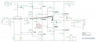
T6 , R11 and R12 is VBE Multiplier
P1 adjust bias current.
T6 is mounted on same heatsink as NPN power transistors T9 and T10
it will thermally track output transistors.
Bias Current for output transistors usually 30ma each
To adjust bias look at schematic " test point 1"
Adjust P1 for 6.5 to 7.2 mV across R19
I made values of resistors so bias is about
right with P1 centered
Still need to measure voltage drop across R19
to confirm.
Attachments
Yes Good, Im glad you figured out the NFB jumpers in my schematic.Thanks White Dragon I Have Seen Your Schematic It Looks Great Everything Perfectly Adjusted I Appriciate Your Work This A Very Good Design Love It... But I Edit Your Schematics Transistors Only According To Me Which I Can Easily Buy Or Available every time here look at the schematic can it be a final version for the schematic so I can build it easily. But I have to give it 35v 35v AC I will add more transistor in it after building it...
I used to make schematic easy to draw.
For amplifier the connection is how you draw.
2SA1015 transistor 50 volt rating
So is ok for differential input / first gain stage
or T1 and T2 50 volt transistor is ok
Second Gain Stage and Current Source
Transistors T3 , T4 and T5
Should not be 50 volt
They should be 80 to 100 volt rating
2SA1015 not good.
I would find similar package easily available to you
with 80 to 100 volt or higher voltage rating.
Have fun
Capacitors C5 , C10, C8 , C9 help stabilize amplifier
mount them as close as possible to transistor
when you make your board
Capacitors C11 , C12 , C13 and C14
also important to stabilize power transistors.
Same idea, very important to mount very close
to NPN power transistors T9 , T10
T6 Thermal Tracks power transistor.
T6 , T9 , T10 all mounted on same heatsink
T1 and T2 differential input / first gain stage
It is good practice and common to want
these transistors to be same temperature.
Mount on board very close together.
Is common to mount flat side to flat side.
Can even bond case to case with zip tie
or heat shrink tube.
Last edited:
2SD313/B507 are only rated for 60 volts. I know, they have been used in commercially available amplifiers (supposedly good ones too) with power supplies as high as +/-75 volts. That’s over 2X rating. If you do not know how to test and select them, DO NOT DO THIS. I wouldnt run one that high either regardless of how it tested. 100V, probably - but ONLY after testing.
Thanks I Am going To Be Print Out Your Shematic Today Then I Will post Here Pic Of Your Own Schematic...Yes Good, Im glad you figured out the NFB jumpers in my schematic.
I used to make schematic easy to draw.
For amplifier the connection is how you draw.
2SA1015 transistor 50 volt rating
So is ok for differential input / first gain stage
or T1 and T2 50 volt transistor is ok
Second Gain Stage and Current Source
Transistors T3 , T4 and T5
Should not be 50 volt
They should be 80 to 100 volt rating
2SA1015 not good.
I would find similar package easily available to you
with 80 to 100 volt or higher voltage rating.
Have fun
Capacitors C5 , C10, C8 , C9 help stabilize amplifier
mount them as close as possible to transistor
when you make your board
Capacitors C11 , C12 , C13 and C14
also important to stabilize power transistors.
Same idea, very important to mount very close
to NPN power transistors T9 , T10
T6 Thermal Tracks power transistor.
T6 , T9 , T10 all mounted on same heatsink
T1 and T2 differential input / first gain stage
It is good practice and common to want
these transistors to be same temperature.
Mount on board very close together.
Is common to mount flat side to flat side.
Can even bond case to case with zip tie
or heat shrink tube.
But I Have Now Only 1 Lil bit Confusion with R12 resistor Value????
Attachments
220m is “Spice” for 0.22 ohms. These resistors are usually a fraction of an ohm. The better your thermal compensation circuit is, and the more closely paralleled outputs match, the smaller they can be. With a proper Vbe multiplier, 0.22 ohms is the right value. If you are paralleling outputs and have concerns about how well matched they are (ie, if they were from different batches) you would increase the resistor value.
Thanks WG_ski now I can Easily use 0.22 Ohm 5 watt resistors220m is “Spice” for 0.22 ohms. These resistors are usually a fraction of an ohm. The better your thermal compensation circuit is, and the more closely paralleled outputs match, the smaller they can be. With a proper Vbe multiplier, 0.22 ohms is the right value. If you are paralleling outputs and have concerns about how well matched they are (ie, if they were from different batches) you would increase the resistor value.
I only buy one value 0.22’s. 100 or more at a time. They get used in everything.
Yesss Yesss You Are Right...I only buy one value 0.22’s. 100 or more at a time. They get used in everything.
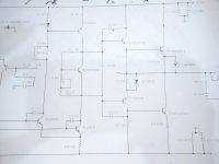
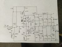
I think this schematic is similar to been developed by Video Rockola in past.Helo Friends I Am Building Class Ab Amplifier Using This Shrmatic Do I Need Some Changes For Better Quality Or for More Watts Outputs???
Thanks In Advance...
Here Is A Shematics..
Also the bias section need improvement. With the present arrangement bias current will surely vary with rail voltage and temperature and it would probably be not possible to keep the bias current within a suitable range. In my openion VAS and driver transistors need to be replaced by better transisstors like KSC 3503 and KSA1381 having very low Cob. I donot think TIP and MJE 340/350 transistors are suitable for VAS.
If you want to build an amplifier with no bias current adjustment with much lower distortion and excellent sonic quality audio, my advice is go for Elvee's Circlophone. https://www.diyaudio.com/community/threads/my-little-cheap-circlophone-c.189599/
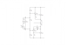
Here is an output stage from a circuit I built years ago. This shows two points:
(1) better symmetry by connecting the resistors on the bases of the output transistors between the base and emitter in both halves
(2) including the "emitter" resistor as I posted previously inside the PNP/NPN feedback loop which will give better stability.
If you need to parallel transistors, then you either have to put the base resistors down to the centre rail or negative rail, accordingly, or add a separate base resistor for each transistor. Naturally this would lower the overall resistance, but that is necessary to maintain the equivalent drive or reverse drive to a single device.
Also, if using parallel devices (and you will need to for higher output powers) add emitter resistors to share the current. That includes keeping the "emitter" resistor in the collector circuit of the lower output NPN device to maintain the input impedance for the Baxandall diode.
If you use 0.33 ohm emitter resistors then the resistor in series with the collector of the lower NPN needs to be 0.33/n, where n is the number of parallel transistors, to keep things symmetrical.
Attachments
Thanks Your Explanation Is Good..Here is an output stage from a circuit I built years ago. This shows two points:
(1) better symmetry by connecting the resistors on the bases of the output transistors between the base and emitter in both halves
(2) including the "emitter" resistor as I posted previously inside the PNP/NPN feedback loop which will give better stability.
If you need to parallel transistors, then you either have to put the base resistors down to the centre rail or negative rail, accordingly, or add a separate base resistor for each transistor. Naturally this would lower the overall resistance, but that is necessary to maintain the equivalent drive or reverse drive to a single device.
Also, if using parallel devices (and you will need to for higher output powers) add emitter resistors to share the current. That includes keeping the "emitter" resistor in the collector circuit of the lower output NPN device to maintain the input impedance for the Baxandall diode.
If you use 0.33 ohm emitter resistors then the resistor in series with the collector of the lower NPN needs to be 0.33/n, where n is the number of parallel transistors, to keep things symmetrical.
Can You Provide Full Circuit Diagram using 2SC5200 Or 2DA1943 As Out Pair Transistors???
Or Using 35-0-35v AC Stereo Diagram
I Mostly Used 35v AC Supply For My All Projects.. In The Past I Was using 24v AC transformer But it did not give me Good Result. The Higher the Power The Higher Output you will get..
I Have Made Many Types Of Amplifiers. Bcoz It is My Passion And Hobby...
In The Past I was Using baxandal Diodes
Bias Control But. It Did Not Gives Good Bias control... Now I use Vbe multimeter trim pots etc for Bias Controlling Thanks.
Want something plug and play, do you? Something that can be built with all junk transistors? The secret sauce to successfully use TIP drivers or anything else equally slow is to use small signal predrivers. I built this a few years back - had to go dig through the archives to find it. The first one used 2N3055 output transistors and ran off a 20-0-20 transformer. Doesn’t sound half bad, and would drive 2 ohms (as in four speakers in parallel) on that power supply. Your supply is a little high for that if you use 3055’s. But with real output transistors - even TIP35’s - it would work. The current limiting will prevent it from running properly on that high a voltage at 2 ohms, but at 4 or 8 it should run fine. I made another later using fake 2SC3281’s and it worked just as well, and didn’t blow up. All unmarked diodes are just 1N4148’s.
Attachments
Thanks A Lot WG-ski You Draw A well Design Of Amplifier But Here Is A Diy Member Name Is White Dragon..Want something plug and play, do you? Something that can be built with all junk transistors? The secret sauce to successfully use TIP drivers or anything else equally slow is to use small signal predrivers. I built this a few years back - had to go dig through the archives to find it. The first one used 2N3055 output transistors and ran off a 20-0-20 transformer. Doesn’t sound half bad, and would drive 2 ohms (as in four speakers in parallel) on that power supply. Your supply is a little high for that if you use 3055’s. But with real output transistors - even TIP35’s - it would work. The current limiting will prevent it from running properly on that high a voltage at 2 ohms, but at 4 or 8 it should run fine. I made another later using fake 2SC3281’s and it worked just as well, and didn’t blow up. All unmarked diodes are just 1N4148’s.
I Requested Him To Make a Schematic For Me which will Use same Npn out Put Transistors...Then After some time He Came Again And He Made A Shematic For Me As My Need.. Many Thanks To Him.. Then I Print Out Diagram. Given By White Dragon..Currently I Am Working On His Given Schematic. I Will Make Amplifier Using This Schematic As Soon As Possible Then Will Post Here.... 🙂
He Design A Well Shematic
For me Here...
https://www.diyaudio.com/community/attachments/vbemods-jpg.1031861/
Last edited:

Sorry been gone, long week at work.Help White Dragon My Bro How Are You??
I Have Another Project With Another Schematic Just Need Your Approval Or Suggestion Is This Good Shematic For As npn pnp Amplifier????
Thanks In Advance...
Here is a Schematic...
I also have received a gift.... a lovely tooth ache. time for dentist
Amplifier posted in post #59
Is very common topology
But is missing a few elements.
Also as noted before, it is using diodes for bias.
This can be done , and does mention they must be mounted
on heatsink to thermal track.
Bias is preset with resistor, so as suggested before is better to make bias adjustable.
Then again most stay away from diode thermal tracking
and I would do same modification as last amplifier.
Would use VBE multiplier and have trimmer potentiometer
for bias adjustment.
Q3 and Q4 is current mirror.
Keeps current balanced for
Q1 and Q2
this will lower distortion and also improve slew rate.
it will also increase open loop gain.
without re writing the book on basic amplifier theory.
C4 value must be correct for stability with changes to open loop gain.
Without calculation, just from experience C4 likely needs to be
slightly larger around 100 to 120p
Q3 and Q4 in schematic do not have degen emitter resistors.
Depending on current set by Constant current source Q5
Emitter resistors need to be added, and the value depends
on current. Your looking for a 60mV to 100 mV voltage drop
across emitter resistors. transistors slightly vary
and is important to have emitter / degen resistors for current mirror
Q5 current source seems to be set low around 600/700 uA
probably about right for GM
But Q6 second gain stage or VAS is simple single transistor.
I would probably raise Q5 current to 2 or 3 mA
Then add degeneration resistors to Q1 and Q2 as well.
To get GM back to where it should be.
But now have extra current overall for Q1 and Q2
to drive 2nd gain stage Q6.
Again without re writing amplifier theory
usually good degen resistor value would be similar
value used for Current mirror degen.
This of course all depends on what the current source
is set to.
with single pair output transistors, very similar to previous
amplifier. suggest around 30 to 35 volts +/-
Last edited:
- Home
- Amplifiers
- Solid State
- Building Class AB Amplifier Do I Need Some Changes??