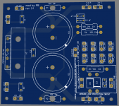
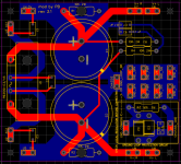
First post contains the latest revision v7.1 of the board. Starting from the second post you can see the process and discussion on how the final version was created.
Relevant discussion on LTspice simulation, CRC PSU type, and general PSU design considerations can be found in this thread - https://www.diyaudio.com/community/threads/need-help-with-ltspice-psus-crc-filter-simulation.386838/
EDITED 11-9-2022
FIXED MAJOR MISTAKE IN THE LAYOUT!!!
Pinout of the LM337 in TO-220 package is not the same as with LM317!
Pin 1 is ADJ for both LM317 and LM337
Pin 2 is IN for LM337
Pin 3 is OUT for LM337
Pin 2 is OUT for LM317
Pin 3 is IN for LM317
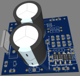
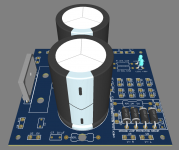
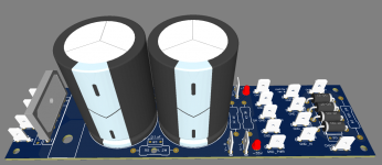
Power supply board was assembled and tested and now comfortably sits in my amp delivering power to two paralleled LM3886 per channel and six opamps (LM4562 and TL052)
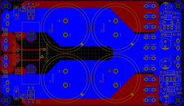
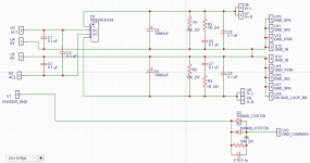
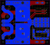
Power supply PCB:
Rectifier bridge - 625-PB3510-E3/45
Heatsink - 490-HSS08-B18-CP
Heatsink pressure clip - 490-HSC-06
Transformer used is Antek AS-4225 (400VA), but AS-3225 (300VA) or AS-2225 (200VA) can be used too.
Gerber files are attached. Great website to make those boards is JLCpcb.
Relevant discussion on LTspice simulation, CRC PSU type, and general PSU design considerations can be found in this thread - https://www.diyaudio.com/community/threads/need-help-with-ltspice-psus-crc-filter-simulation.386838/
EDITED 11-9-2022
FIXED MAJOR MISTAKE IN THE LAYOUT!!!
Pinout of the LM337 in TO-220 package is not the same as with LM317!
Pin 1 is ADJ for both LM317 and LM337
Pin 2 is IN for LM337
Pin 3 is OUT for LM337
Pin 2 is OUT for LM317
Pin 3 is IN for LM317
Power supply board was assembled and tested and now comfortably sits in my amp delivering power to two paralleled LM3886 per channel and six opamps (LM4562 and TL052)
Power supply PCB:
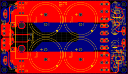
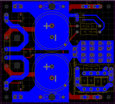
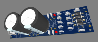
- Space for four 10,000 uF capacitors.
- Space for +/- 15V regulators based on LM317 and LM337.
- Regulators have a space for 0.1uF decoupling capacitors right next to them.
- Space for bleeder resistors and/or LEDs.
- Rectifier bridge used is Vishay PB3510-E3/45 rated at 35A and 1KV. PCB has a space for the rectifier heatsink.
- Space for the snubber capacitors for each of the transformer coil.
- Space for MOV that limits power on voltage spikes. MOV MOV-14D101KTR voltage rating is 60 VAC - that is 10V over the total voltage of the transformer second 25V+25V=50V.
Rectifier bridge - 625-PB3510-E3/45
Heatsink - 490-HSS08-B18-CP
Heatsink pressure clip - 490-HSC-06
Transformer used is Antek AS-4225 (400VA), but AS-3225 (300VA) or AS-2225 (200VA) can be used too.
Gerber files are attached. Great website to make those boards is JLCpcb.
Attachments

Last edited:

I suggest you have a look at the power supply design pcb on Tom Christianson's 'Neurochrome" website called Power-86 - it is very simple and if Tom Christianson considers this adequate for his very well designed amplifiers ....,
In my opinion, those 1N5806 need to be substantially upgraded and/or separated as they'll get extremely hot next to each other - I suggest the soft recovery types like MSR860 (especially as you are charging the 2 x 10,000uF caps) or use a good quality block bridge. The individual diodes might need space for cooling and/or heatsinks, particularly if you're intending to operate the amplifier at elevated power. I would suggest you not use a capacitor bipass on each diode but ....
If you are going to keep the 2 caps, I suggest you add a small value power resistor between (0.1R - 0.5R) to act as a C-R-C supply (reduces supply voltage ripple) and place these on the outside edges of the pcb for better cooling.
Apart from the pcb design layout (larger gaps on the pcb pour for the small donuts, temperature relief for the larger ones, for example), the performance of these simple amplifiers is still dependent on the quality of the power supply so don't skimp on cheap bridges and/or capacitors.
You must be new to power supplies?
1. You just need a single bridge rectifier for the dual voltage supply, but it needs to use larger diodes. I would use a 10A module. You could use a 25A module but 10A is probably enough. Wire the two transformer secondaries as a center tapped winding, the center tap to ground.
2. Sometimes a bridge module is wired like your ground lift because there are 4 diodes in the module, but you only need two. If you are using single diodes, there is no reason to use 4 diodes.
3. 100nF caps on the rectifier diodes is excessive. Doing this has caused noise for me so I wouldn't do it at all, but if you do, 10nF would be the largest caps I would use.
4. If you are going to bother with bleed resistors, why not run that current through red (for +) and ~green (for -) LEDs? It may be useful diagnostics and it looks cool.
Attachments
Adding snubber caps across soft recovery rectifiers is a contentious subject for many diy people but adding the Hagerman snubber network across the transformer secondary winding will achieve a small improvement - If you design them in, you can play with them later. Technically, if you want to add the 100nC film caps across the diodes, you should include the series low value resistor, but this seems to be forgotten these days - individually, these small things are probably inaudible on the 3886, but it's worth considering them.
Now, just arbitrarily adding a film cap to all the electro caps is asking for trouble with high freq resonances, etc and they contribute little, if anything' to a 'better sound' - (again, my opinion, many will disagree) - you still see this designed into many power supplies these days but a far better result can be obtained by just adding a small value high quality electro cap instead such as a 47uF, etc - you can do this later underneath across the main cap's terminals.
You can just use a 50v electro cap here as the 3886 runs power rails around +/- 30v, yes?
Now something more serious to consider - the program appears to want to fill all available 'free' pcb area with copper (less etching required), but, (and a big but too!), to solder in the main caps, you'll need to apply an enormous amount of heat as the large copper areas adjacent the cap's terminals just suck it away and you end up cooking the caps unnecessarily - in your design program, there should be something called thermal relief pads, or something similar.
The second 'downer' is that if you ever want to change the main caps (say 10mF to 22mF CDE or maybe to Mundorf, etc) it'll be a real battle and probably also pull out the sleeve/print-through between the top/bottom copper - a most irritating problem to find!
I hope this 'natter' is of some benefit - I found that using an extra input stage (or impedance buffer) to all the various chip amps was essential and especially if you're using them in 'current gain' or trans.
Thank you all for your input!
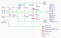
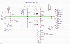
Rev 2.1:
I used EasyEDA editor - just for those who was wondering.


Rev 2.1:
- Removed 0.1 uF caps next to rectifier diodes
- Removed unnecessary diodes from ground loop protection circuit
- Soldering pads on copper plains were replaced with spoke type for better heat management when soldering
I used EasyEDA editor - just for those who was wondering.
Attachments
Now, just arbitrarily adding a film cap to all the electro caps is asking for trouble with high freq resonances, etc and they contribute little, if anything' to a 'better sound' - (again, my opinion, many will disagree) - you still see this designed into many power supplies these days but a far better result can be obtained by just adding a small value high quality electro cap instead such as a 47uF, etc - you can do this later underneath across the main cap's terminals.
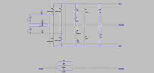
Are you talking about C4, C6, and C3, C10?
That's sorted out the donuts - looking good - this is the 3rd version so I suggest you put a number on it - I just add the date and any different version on that day - it's so confusing later on to remember which version was the final version and what component numbers are changed.
About your caps, you have the main filtering cap C2 (10mF), bipassed by C3 (1uF) and this further bipassed by C1 (0.1uF) - a lot of people say this is 'the way to go' and you'll end up with good results - I'd suggest you leave them there but keep in mind to just try to leave off the 1uF and the 0.1uF and used something like a good quality 47uF instead - people do argue fanatically about this so I'll just say, try it for yourself...
For the output snubber I've forgotten the value but I think it was something like 100nF - 560 in series with the 1R resistor - you might have a look at an old thread about this with Carlos Muchado ("CarlosFM" or "snubberized power supply") - it was back nearly 20 years ago and became a really 'hot topic' even tho it just required people to just add the simple 1R + 560nF (to each rail) across the basic power supply output pins - the 1R0 resistor stays the same and vary the capacitor value.
Something else occurred to me too - there's something like a 220nF cap across the + to - rail at the chipamp's pins - it made quite a difference - Burson V6 discrete ICs use the same idea today.
About C4 and C6 across the secondary windings - there's a whole thread about this called
It's a pretty simple assembly of parts but requires specific cap values - not sure if it'll effect the chipamp's sound but well worth looking up - here the capacitors stay the same and the resistor varies depending on the actual transformer - there should be a specific value posted for your transformer somewhere in the thread as people were reporting the values.
For the main filtering capacitor, the 10mF ones, purchase the best quality that the budget allows - it does make an considerable difference.
About your caps, you have the main filtering cap C2 (10mF), bipassed by C3 (1uF) and this further bipassed by C1 (0.1uF) - a lot of people say this is 'the way to go' and you'll end up with good results - I'd suggest you leave them there but keep in mind to just try to leave off the 1uF and the 0.1uF and used something like a good quality 47uF instead - people do argue fanatically about this so I'll just say, try it for yourself...
For the output snubber I've forgotten the value but I think it was something like 100nF - 560 in series with the 1R resistor - you might have a look at an old thread about this with Carlos Muchado ("CarlosFM" or "snubberized power supply") - it was back nearly 20 years ago and became a really 'hot topic' even tho it just required people to just add the simple 1R + 560nF (to each rail) across the basic power supply output pins - the 1R0 resistor stays the same and vary the capacitor value.
Something else occurred to me too - there's something like a 220nF cap across the + to - rail at the chipamp's pins - it made quite a difference - Burson V6 discrete ICs use the same idea today.
About C4 and C6 across the secondary windings - there's a whole thread about this called
Simple, no-math transformer snubber using Quasimodo test-jig
organized by Mark Johnson - the first post in that thread about 10 years ago is quite descriptive and details what secondary transformer windings plus diodes actually do and introduces the well known Hagerman snubber technique.It's a pretty simple assembly of parts but requires specific cap values - not sure if it'll effect the chipamp's sound but well worth looking up - here the capacitors stay the same and the resistor varies depending on the actual transformer - there should be a specific value posted for your transformer somewhere in the thread as people were reporting the values.
For the main filtering capacitor, the 10mF ones, purchase the best quality that the budget allows - it does make an considerable difference.
4. If you are going to bother with bleed resistors, why not run that current through red (for +) and ~green (for -) LEDs? It may be useful diagnostics and it looks cool.
What LEDs can I install there?
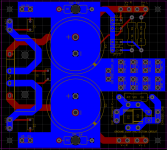
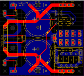
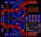
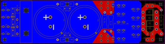
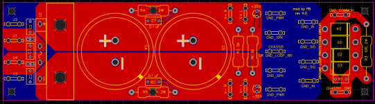
Revision 3.0:


Gerber files and screenshots attached.
- Replaced rectifier diodes with 35A 800V bridge - Mouser part 625-PB3508-E3/45 by Vishay
- Added heatsink for the bridge - Mouser part 490-HSS08-B18-CP
- Redesigned ground plane to be T type
- Bleeder resistors are increased to 10K, mounted on the edges of PCB, have holes for airflow from beneath
- Added space for optional caps for filtering RF
- C4, C5 are Nichicon caps with properly sized soldering pads now
Gerber files and screenshots attached.
Attachments
Last edited:
1. Unless you are using this for a Kilowatt amplifier, the rectifier heatsink is likely unnecessary.
2. The layout is fine but the schematic shows the ground link some distance from the bulk caps. Be aware that any trace resistance between the two bulk caps is a bad thing. See "star grounding". Each ground, especially the transformer, should not share a path with the other ground connections to the center point between the two bulk storage caps.
https://www.analog.com/en/analog-dialogue/articles/staying-well-grounded.html
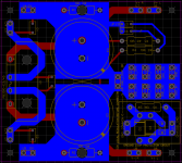
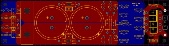
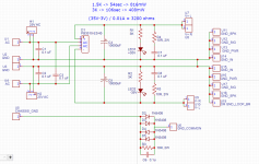
Revision 3.1:

Gerber files attached
List of parts PDF attached
- Split up ground between two caps
- Removed unnecessary filtering caps
- Fixed resistance value to 10R
- List of parts in PDF
Gerber files attached
List of parts PDF attached
Attachments


Last edited:
Revision 3.2:
- Added two more diodes to ground loop protection to double the current handling to 6A in each direction
Attachments
Another revision - relocated snubber RC networks to be closer to the 10,000uF caps. Added LEDs to discharge resistors to be able to indicate separately + and - 35V supply status.
Resistors were calculated based on LED voltage drop of 1.2V and current of 5mA. R = (35V-1.2V) / 0.005A = 6,760 ohms. With 5.6kOhm we have 33.8/5.6=6.03 mA current supplied.
Increased size for PCB traces to 8mm
Resistors were calculated based on LED voltage drop of 1.2V and current of 5mA. R = (35V-1.2V) / 0.005A = 6,760 ohms. With 5.6kOhm we have 33.8/5.6=6.03 mA current supplied.
Increased size for PCB traces to 8mm
Attachments
-
 Screen Shot 2022-03-27 at 12.23.23 AM.png51.2 KB · Views: 226
 -
 Screen Shot 2022-03-27 at 12.24.58 AM.png46.8 KB · Views: 198
 -
 Screen Shot 2022-03-27 at 12.27.15 AM.png24.4 KB · Views: 183
 -
 Screen Shot 2022-03-27 at 12.38.22 AM.png70 KB · Views: 169
 -
Gerber_psu-bridge-pcb_2022-03-27.zip40 KB · Views: 101
In this revision here I resized the board to be 170mm by 45mm as this is requirement because of the case that I have. Fine tuned resistor for LED based on 3V drop and 10mA current - 3.2k value, 400mW rating min. Added headers to tap into 25V AC to use that for fast turn off protection board.
Attachments
I frequently deploy a C+RC snubber across each transformer secondary, where Cx=Cacross is implemented as an MOV (metal oxide varistor) instead of a capacitor. The MOV (a) is about the same cost; (b) can be Quasimodo-optimized for critical damping just like a capacitor, and (c) adds an extra layer of surge protection, for free. To see one example, search the Forums for threads with "VRDN" in the title.
- Home
- Amplifiers
- Power Supplies
- LM3886 power supply