Referring to the datasheets: The 846/56 PN variant is at EOL or end of life status but both those and the The BCM846/56 types are specified as precision matched with <+/-10% difference in hFE and Vbe between each transistor in the pair over a range of low current levels. Those are worst case numbers and still pretty good for production parts because those numbers will be much better in reality.
I'm having trouble with posting links at the moment but you only have to type into your browser the full transistor part number followed by "datasheet", or "datasheetcatalog", which is my preference of website for picking whose datasheets I want to read. Nexperia and
Infineon's websites will have links to their current product and datasheets in any case.
Yes, desoldering can sure do damage with SMDs. I don't do much if I can help it because you need 3 hands but there are ways of using 2 irons and little U shaped tips to heat 2 or more points simultaneously but that needs a chunk or two of copper and fettling to make something useful.
Okay, thats good to know the BCM846/56 are precision matched. Thanks for the wider net search tip. I'm thinking of using the SOIC8 adapters and solder wire directly to the SMD pads. Is that advisable? On the other hand, I have single 10 BC846Bs and 10 BC856Bs. I don't have a setup to match the pairs. From what I can gather in my reading, there are circuits where matching isn't so critical because the mismatching is cancelled out by negative feedback. Could that be the case in my circuit?

Last edited:
Negative feedback comes in local and global flavors. Local feedback is usually only a modest amount that exploits an existing circuit arrangement in order to reduce isolated linearity problems. However, the 2 LTPs here are mirrored devices which differentiate the input and (suitably scaled) output signals. They work alternately in the positive and negative swings of the input signal to produce a differentiated signal that should result in a corrected output signal. Consequently, the output level is maintained according to that scaling too - about 50:1 here. Therefore, it's global feedback that controls the primary function of the amp and is a cornerstone of the design.
It's an interesting point that feedback being an idealised correcting mechanism, should make everything better etc. but we've been discussing particular semis that may do this job better than others. I think this means that nothing real is really perfect and neither is feedback in real circuits so assuming simple theory holds true in all respects is at best risky. I'm guessing by the reference you made to uncritical matching that the writer had a particular design or type of amp in mind because some designs are so critical as to be near impossible to adjust and use even with the specified parts. When we don't have the training or field experience to know what the best approach in our particular application is going to be and how to verify it, I think it is going to be much safer to go with the original designer's plan, which it's worth noting, is based on the Creek 5350 design by the look of it - that service manual or at least its schematic might be worth reading for background.
As to wiring up the adapter boards, I guess it comes down to convenience but the boards are a sensible approach when you haven't tackled this size of work before. I do mostly through-hole projects and that leaves me with a lot of short lengths of tinned steel and copper wire. I pick these up with square-nosed mini pliers, bend one end into a very short elbow and solder the bent part to the pad in a quick sequence. Then I try to make direct, vertical connections to the board without crossing legs or shorting anything because cheap heatshrink tubing won't stand fiddling about with a hot iron. Fit tubing if you have some tiny stuff and line up the wires to the adapter holes and hope to goodness you have the right sequence of wires when you do this - it can get messy if you need to cross them over when it doesn't work.
You've probably come across threads where this little parts testing beauty comes up for discussion. If you want to match transistors for the basic hFE, Vbe parameters, this one's a pleasure to use. It tests a lot of other things too and is USB rechargeable but take care with transistor temperatures - allow them to normalise to room temp. or measurements will drift until they do.
disclaimer - just the words of a happy customer with no interest in selling anything)
This is one of many sellers: https://www.amazon.com/Longruner-Po...words=transistor+tester&qid=1639808055&sr=8-3
Thank you for the insight and link to the multi-function tester. I'm just now reading about differential signals. I think I see the following transistors in the input stage: 1 pair of NPN, 1 pair of PNP, and 2 pairs of complementary NPN/PNP which are complementary LTPs, correct? Then there's one pair of complementary transistors BF622 and BF623 that follow the 2 LTPs. It seems like the focus has been on the LTPs but I don't know how important matching is for these other transistors before and after the LTPs. Regarding the dual transistor adaptor: I think I'll stick with single transistors instead of building an adaptor rig and trying to fit that in an already tightly spaced PCB, also first time mistakes might be too risky. temperature sensitivity is duly noted which might require more work to connect probes to the smd leads. My fingers will probably quickly add 30 degrees F! How many transistors would you recommend bulk buying to pick out each well matched pair? I wasn't able to glean more information from the 5350 schematic, and didn't find the service manual. If I replace the input transistors what's the worst and best case scenario I should anticipate? Is there much data on other hobbyist and diyers hearing a marked sound quality improvement? Are there before and after measurements that can match the subjective and objective differences? I found this article but will need to read it again several more times and learn before seeing how it overlaps with our conversation. https://www.eetimes.com/distortion-in-power-amplifiers-part-ii-the-input-stage/Negative feedback comes in local and global flavors. Local feedback is usually only a modest amount that exploits an existing circuit arrangement in order to reduce isolated linearity problems. However, the 2 LTPs here are mirrored devices which differentiate the input and (suitably scaled) output signals. They work alternately in the positive and negative swings of the input signal to produce a differentiated signal that should result in a corrected output signal. Consequently, the output level is maintained according to that scaling too - about 50:1 here. Therefore, it's global feedback that controls the primary function of the amp and is a cornerstone of the design.
It's an interesting point that feedback being an idealised correcting mechanism, should make everything better etc. but we've been discussing particular semis that may do this job better than others. I think this means that nothing real is really perfect and neither is feedback in real circuits so assuming simple theory holds true in all respects is at best risky. I'm guessing by the reference you made to uncritical matching that the writer had a particular design or type of amp in mind because some designs are so critical as to be near impossible to adjust and use even with the specified parts. When we don't have the training or field experience to know what the best approach in our particular application is going to be and how to verify it, I think it is going to be much safer to go with the original designer's plan, which it's worth noting, is based on the Creek 5350 design by the look of it - that service manual or at least its schematic might be worth reading for background.
As to wiring up the adapter boards, I guess it comes down to convenience but the boards are a sensible approach when you haven't tackled this size of work before. I do mostly through-hole projects and that leaves me with a lot of short lengths of tinned steel and copper wire. I pick these up with square-nosed mini pliers, bend one end into a very short elbow and solder the bent part to the pad in a quick sequence. Then I try to make direct, vertical connections to the board without crossing legs or shorting anything because cheap heatshrink tubing won't stand fiddling about with a hot iron. Fit tubing if you have some tiny stuff and line up the wires to the adapter holes and hope to goodness you have the right sequence of wires when you do this - it can get messy if you need to cross them over when it doesn't work.
You've probably come across threads where this little parts testing beauty comes up for discussion. If you want to match transistors for the basic hFE, Vbe parameters, this one's a pleasure to use. It tests a lot of other things too and is USB rechargeable but take care with transistor temperatures - allow them to normalise to room temp. or measurements will drift until they do.
disclaimer - just the words of a happy customer with no interest in selling anything)
This is one of many sellers: https://www.amazon.com/Longruner-Po...words=transistor+tester&qid=1639808055&sr=8-3
and yes ultimately this is about enjoying the music, correct lol?
Last edited:
I found a tester for smd transistors.
https://www.amazon.com/gp/aw/d/B07WT9VVZB?ref=ppx_pt2_mob_b_prod_image
https://www.amazon.com/gp/aw/d/B07WT9VVZB?ref=ppx_pt2_mob_b_prod_image
Yes, that model has a contact pad for testing common size, like SOT-23, single SMD transistors. Unfortunately, it has 3 reviews that are all bad and may be why it's unavailable here, at least. There is another model that's well set up for testing single SMD transistors and comes in a maroon or black case but it has the worst, lowest contrast LCD screen imaginable. https://www.amazon.com/BSIDE-ESR02-...words=transistor+tester&qid=1640046325&sr=8-9
There aren't any choices for testing dual SMD transistors because the contact pad arrays would need configuring for each pinout type and these ATmega328 based testers couldn't auto-sense them anyway.
I use the mini hook probes that usually can be re-shaped to clip onto the tiny legs without shorting but the alloy is brittle - it doesn't like repeated bending. The hooks vary and some aren't all that "mini" so you may need to do some adapting of your own.
You've raised a lot of other questions and some deserve a bit more than a casual reply. I'll have to do some digging myself but for starters, the EEtimes article is an extract from Douglas Self's "Audio Power Amplifier Design Handbook" now in its 6th edition but the 4th ed. has been on the net for free download for some years now so I leave it to you to google, rather than add a download link that may bend the rules. It has similar basic content but is generally easier to read than later editions, for editorial reasons, I think.
Regarding matching, you'll only see benefit from matching the LTP transistor pairs Q102/3 and Q107/8, already discussed. I'm guessing the other channel references are Q2/3 and Q7/8 which would be conventional numbering. These are described as galvanicly isolated pairs so there could be something in selecting particular pairs but I doubt you'll hear more than an illusory sonic benefit, as I found long ago, even with Natsemi's LM394 supermatched pairs. There just isn't much point selecting a particular pair from those that are already sufficiently well matched by the manufacturing process. Generally, it's is a waste of time where global feedback controls the overall gain and normal, close component tolerances take care of local differences which goes some way towards answering your remaining questions on feedback. Whilst this search for precise matching at audio frequencies goes on though, we also have to be concerned about DC balance or offset, too. That's yet another layer of priorities and often conflicting solutions.
Where multiple transistors are in parallel, such as the output transistors of a big amplifier, matching is often required there to ensure optimum stable performance and current sharing at maximum power level. It's an expensive but necessary way to maintain stable and reliable high power for PA, live music reinforcement and is usually a pro. audio application but there are monster home theatre systems out there too - a power trip that some people find compelling in itself.
Yes, that model has a contact pad for testing common size, like SOT-23, single SMD transistors. Unfortunately, it has 3 reviews that are all bad and may be why it's unavailable here, at least. There is another model that's well set up for testing single SMD transistors and comes in a maroon or black case but it has the worst, lowest contrast LCD screen imaginable. https://www.amazon.com/BSIDE-ESR02-...words=transistor+tester&qid=1640046325&sr=8-9
There aren't any choices for testing dual SMD transistors because the contact pad arrays would need configuring for each pinout type and these ATmega328 based testers couldn't auto-sense them anyway.
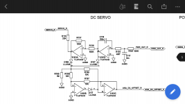
I think you mean Q101/2 and Q106/7 make up the LTPs, correct? Your details help put matching LTP transistors in this circuit into perspective, thanks. I am in the dark here but can gather sound quality improvements are unlikely. It will take some time for me to piece things together. For instance, is the DC Servo part of the global feedback you mention? I understand it reduces dc offset and appears to do this recursively. Which brings up another potential reason to replace the LTPs: I believe I’m seeing a larger channel imbalance in the right channel. The DC Servo circuit at U101 pin 1 =80mV, vs. U1(1)=15mV in the left channel. Am I correct in my interpretation ? If so, can replacing the LTPs with better matched pairs improve the channel balance? Does that spill over as dc offset? Also, I’m seeing the dc servo output - U101 (8 and 9) = 80mV that slowly reduces to 20mV after warming up. While measuring at trh speaker posts is less than 1mV. Versus left channel U1 (8 and 9) is less than 1 mV. Sorry for the tangent.Yes, that model has a contact pad for testing common size, like SOT-23, single SMD transistors. Unfortunately, it has 3 reviews that are all bad and may be why it's unavailable here, at least. There is another model that's well set up for testing single SMD transistors and comes in a maroon or black case but it has the worst, lowest contrast LCD screen imaginable. https://www.amazon.com/BSIDE-ESR02-...words=transistor+tester&qid=1640046325&sr=8-9
There aren't any choices for testing dual SMD transistors because the contact pad arrays would need configuring for each pinout type and these ATmega328 based testers couldn't auto-sense them anyway.
I use the mini hook probes that usually can be re-shaped to clip onto the tiny legs without shorting but the alloy is brittle - it doesn't like repeated bending. The hooks vary and some aren't all that "mini" so you may need to do some adapting of your own.
You've raised a lot of other questions and some deserve a bit more than a casual reply. I'll have to do some digging myself but for starters, the EEtimes article is an extract from Douglas Self's "Audio Power Amplifier Design Handbook" now in its 6th edition but the 4th ed. has been on the net for free download for some years now so I leave it to you to google, rather than add a download link that may bend the rules. It has similar basic content but is generally easier to read than later editions, for editorial reasons, I think.
Regarding matching, you'll only see benefit from matching the LTP transistor pairs Q102/3 and Q107/8, already discussed. I'm guessing the other channel references are Q2/3 and Q7/8 which would be conventional numbering. These are described as galvanicly isolated pairs so there could be something in selecting particular pairs but I doubt you'll hear more than an illusory sonic benefit, as I found long ago, even with Natsemi's LM394 supermatched pairs. There just isn't much point selecting a particular pair from those that are already sufficiently well matched by the manufacturing process. Generally, it's is a waste of time where global feedback controls the overall gain and normal, close component tolerances take care of local differences which goes some way towards answering your remaining questions on feedback. Whilst this search for precise matching at audio frequencies goes on though, we also have to be concerned about DC balance or offset, too. That's yet another layer of priorities and often conflicting solutions.
Where multiple transistors are in parallel, such as the output transistors of a big amplifier, matching is often required there to ensure optimum stable performance and current sharing at maximum power level. It's an expensive but necessary way to maintain stable and reliable high power for PA, live music reinforcement and is usually a pro. audio application but there are monster home theatre systems out there too - a power trip that some people find compelling in itself.
Last edited:
Also thanks for the link. I went ahead and ordered that tester. At the least it will be fun checking hFE and Vbe values 🙂.I’ll try and use a rubber-band to fasten the transistor to the test pad.
Last edited:
Yes, correct. I took that 6 for an 8, when reading Q106. The little numbers are somewhat blurred on my screen.
DC offset is treated more seriously with Mosfet amplifiers like this later, Creek design. The actual circuit for the DC servo must be on another schematic but we can see that the servo connects to the same node as the audio negative feedback loop, at the bases of Q102 and 106 of the input LTPs . The servo itself is usually a JFET type IC opamp or two in a circuit that filters out the audio signal in order to sample just the averaged DC potential or "offset" at the amplifier output, WRT signal ground. It then servos out that averaged error by adjusting the dc potential at the LTP accordingly. Again, there will be a scaling factor according to the amplifier's gain but this time its DC gain, not the same as its AC or audio signal gain.
For testing single SMD transistors on the contact pad, just push down on the semi gently with an eraser pencil or softwood stick - much easier and faster than clamping it somehow.
Last edited:
Ah ok Im understanding more on how the input transistors are connected to the dc servo, and why there are diodes in the dc servo in the first place. BTW the dc servo circuit is located on pages 4 and 5 on the main board schematic I uploaded. Does the 80mV wrt ground at U101(1) represent the channel imbalance between the signals? ok an eraser sounds like an easier method, thanks.Yes, correct. I took that 6 for an 8, when reading Q106. The little numbers are somewhat blurred on my screen.
DC offset is treated more seriously with Mosfet amplifiers like this later, Creek design. The actual circuit for the DC servo must be on another schematic but we can see that the servo connects to the same node as the audio negative feedback loop, at the bases of Q102 and 106 of the input LTPs . The servo itself is usually a JFET type IC opamp or two in a circuit that filters out the audio signal in order to sample just the averaged DC potential or "offset" at the amplifier output, WRT signal ground. It then servos out that averaged error by adjusting the dc potential at the LTP accordingly. Again, there will be a scaling factor according to the amplifier's gain but this time its DC gain, not the same as its AC or audio signal gain.
For testing single SMD transistors on the contact pad, just push down on the semi gently with an eraser pencil or softwood stick - much easier and faster than clamping it somehow.
Attachments
Last edited:
Err I think understand…Ah ok Im understanding more on how the input transistors are connected to the dc servo, and why there are diodes in the dc servo in the first place. BTW the dc servo circuit is located on pages 4 and 5 on the main board schematic I uploaded. Does the 80mV wrt ground at U101(1) represent the channel imbalance between the signals? ok an eraser sounds like an easier method, thanks.
Well I replaced the right channel LTPs.Err I think understand…
I tested each transistor at least 3 times for consistency. Finding 2 matches was surprisingly easy out of 15 bc856b and 15 bc846b. Matched hFE gain values were within 2% ( the full hFE range of tested transistors was 275-330) And matched Vbe within 5% ( range 660-720). As it turns out U101(8 and 9) increased from 20mV to 200mV with the newly matched transistors. Is this 200mV something to be concerned about? However dc offset at the speaker terminals is still well below 10mV. What I don’t understand is why the dc offset output value increased with these well-matched pairs. Anyhow, I’ve learned my lesson don’t fix it unless it’s broken, and fortunately I’m still ahead - the amp still works and still sounds good to my ears.
Last edited:
Ok reading your post again regarding the dc servo. It looks like the dc servo is doing its job just fine. For anyone who decides to replace these ant-sized transistors in tight spaces I found the easiest removal method is add a small amount of solder to each lead and then use a fluxed desoldering braid back and forth until the transistor slides off. Clean up, then slide the new transistor onto a heated small puddle of solder for the collector lead. I added solder to the remaining leads with the nail polish method. Just a wee bit on the solder tip and then painting that on the leads. And just to follow up any changes to sound characteristics before and after swapping the input transistors are imperceptible. Thanks again for all the help!
I'm still curious about out why the dc servo is seeing 300mV (a 4x voltage gain compared with stock bc846b and bc856b) at U101 pin 1 WRT ground. Is the initial offset before the dc servo? Could it be caused by poorly matched LTPs? It turns out the the tester is inconsistent (within 10%) when reading bc846b hFE values: It switches from 284 to 301 hFE, while Vbe values are consistent. hFE values for the bc856bs are consistent (within 1%). Is it possible under-matched NPN/PNP LTPs (yet still within 10%) explain the increase in voltage at U101 pin 1? Or what might cause such an apparent big rise in voltage (80mV to 300mV) at U101 pin 1? Thanks for any help.
Last edited:
Or did Creek Audio bulk-buy very well matched complementary pairs? Wouldn’t hand picking matched pairs for each amp be extraordinarily costly? It seems like I’m missing a glaring mistake here.
'Good that you've worked your way through most troubles by your own reasoning and resolution.
I didn't give this much thought with my tester that's like your new BSIDE one, but the typical smallest increment in hFE reading is 7% here. hFE is the result of comparing the step size of current applied to the base with the resulting increase in collector current, all controlled by the the firmware in the tester's microprocessor. That's another story but its a fast and repeatable technique, adequate for matching purposes. However, I doubt very much that the Destiny amplifier or any other mass-produced model would have incorporated hand selected, closely matched components. That sort of feature is in the very expensive, custom parts end of the market but I admit that there is adifference with closely matched semis. I just don't think its necessarily an improvement to musical entertainment.
To illusrate what's normal now in cheap, hobby parts, I just used my TC-1 tester (suggested in #23) with a bag of 100 generic BC550C (high gain-low noise types in a thru-hole T092 package). A sample of 10 of these measured 430-470 with several bang-on 431hFE. Not bad, assuming it's accurate but there looks to be a little grouping effect in a larger lot size, perhaps a consequence of the incremental test currents .
I believe the discrete semis in production now, are considered consistent and matched well enough by virtue of modern, large wafer manufacturing processes and automated assembly. We use those semis, as they come in the sequence of their bandolier packing, which gets stripped from the device in the assembly process. That's not much different to how I ensure a good match when I repair an input stage or preamp. The significant issue with hFE measurement though, is temperature - don't touch or breathe on them if you want to measure anything critical.
Small signal, discrete transistors are only worth matching if they can be maintained at the same temperature within just a few degrees C. This is mostly affected by the PCB layout and location relative to heat sources and ventilation. Some manufacturers even go to great lengths to both couple and isolate the input LTP(s) from the effects of heat because the bias and signal currents will fluctuate and drift throughout the temperature cycles of normal use. Even when you really turn up the volume, the sound can audibly change for a number of reasons but thermal lag would be among them. Even so, dual packages will outperform discrete pairs any time.
I've been thinking about your determination to change the LTP transistors and I've read the comments in other posts here which naysaid the idea. Sometimes it's good to let people find out for themselves why it's better to trust the design engineer rather than trying to satisfy your urges to change things because you can or try to fix them if they seem to be broken. It's quite a blow to have to sideline a project because we don't see a way forward once the enthusiasm begins to wane. To me, it's the kid in the candy store syndrome - I've got a sweet tooth too or at least had one that keeps me taking on projects that will probably take another lifetime to get around to enjoying. That doesn't stop me but when I rendered useless a friend's perfectly good Technics amplifier (I assumed it would be a convential class AB amp. but couldn't locate a manual that covered it.) I should have stopped and thought about why I kept on tinkering with something that was fried and wasn't going to work again until the special power transistor and heatpipe assemblies were replaced or expertly rebuilt, if that was possible.
Trouble also begins when someone sparks our interest in modifying stuff for the hell of it. When we realise that buying parts is pretty simple nowadays, we're encouraged to dive in and learn things as fast as we can, so that we can get started real soon. This is great but when we find the way to modify stuff successfully is a lot harder that building a successful clone from scratch even, it does put a damper on the fire. The Destiny amp is quite a highly regarded piece of electronics as it was designed and unless you see it otherwise, I'd try to retore what was working with the original semis before you forget where the orinal parts were located - i.e. ASAP.
Once its working again, is when to think about what went wrong and straighten out the plan.
Input transistors are probably matched. A typical input diff amp, CCS, current mirror, the gain is irrelevant. I would not be looking at the input doe DC instability.Hi,
Thanks for the response. What is the harm in replacing those transistors if at least for the sake of inexpensive preventative maintenance? I've already replaced all the diodes and electrolytic caps. I've also cleaned more of the burned flux. I am suspicious there is an issue in the right channel because dc offset is very jumpy after warming up (I've replaced the dc servo components), yet still below 10mV. The amp has a long history of damage from yours truly, I've shorted some components, over biased the output devices etc. It also an unknown history and bought for parts. I am trying to find out in this particular circuit will there be a sonic difference between using lower gain (~220) transistors which are stock in my case, or the higher gain (~420) ones that are in the schematic, and the other Destiny.
Thans for your responses. Yes, I had the exact same thought of a kid in a candy store looking at those dual non/pnp transistors last night and envisioning how a SOIC to DIP adaptor might work. Looking back I wouldn't change them again but yes its also was fun to work on the amp and good to learn these things. Unfortunately I lost or damaged the original semis, and there was a learning curve in removing them. Fearful of sound quality changes I tried a crude approach of testing for non-linear gain by using an online waveform generator with odd and even harmonic sliders, record the output through each speaker at the same distance and height, and then running a FFT analysis on Audacity to check for any left vs right channel trends inharmonic distribution. As it turns out I could not find a trend where some harmonics are more amplified more than others aside from one speaker oddly reducing some harmonics. I also verified dc voltages across R103/4 and R146/7 are very close to R3/4 and R46/7 at around 70mV.I've been thinking about your determination to change the LTP transistors and I've read the comments in other posts here which naysaid the idea. Sometimes it's good to let people find out for themselves why it's better to trust the design engineer rather than trying to satisfy your urges to change things because you can or try to fix them if they seem to be broken. It's quite a blow to have to sideline a project because we don't see a way forward once the enthusiasm begins to wane. To me, it's the kid in the candy store syndrome - I've got a sweet tooth too or at least had one that keeps me taking on projects that will probably take another lifetime to get around to enjoying. That doesn't stop me but when I rendered useless a friend's perfectly good Technics amplifier (I assumed it would be a convential class AB amp. but couldn't locate a manual that covered it.) I should have stopped and thought about why I kept on tinkering with something that was fried and wasn't going to work again until the special power transistor and heatpipe assemblies were replaced or expertly rebuilt, if that was possible.
Trouble also begins when someone sparks our interest in modifying stuff for the hell of it. When we realise that buying parts is pretty simple nowadays, we're encouraged to dive in and learn things as fast as we can, so that we can get started real soon. This is great but when we find the way to modify stuff successfully is a lot harder that building a successful clone from scratch even, it does put a damper on the fire. The Destiny amp is quite a highly regarded piece of electronics as it was designed and unless you see it otherwise, I'd try to retore what was working with the original semis before you forget where the orinal parts were located - i.e. ASAP.
Once its working again, is when to think about what went wrong and straighten out the plan.
And I'm seeing very good dc offset voltages at the right speakerr terminals: 1-3mV. I'm not hearing any issues in the right speaker either.
But should I be concerned about the numbers I'm seeing in the Right DC Servo WRT the left? If so, what troubleshooting steps would you recommend to identify the issue(s)?
U101 pin 1: ~300mV (formerly 80mV) ; U1 pin 1: ~15mV
U101 pin 8 and 9: ~150mV (formerly 20mV); U1 pin 8 and 9: ~0.6 mV
The original semi were also BC856B and BC846B, I can't figure out why those numbers changed with perhaps better matched pairs.
- Home
- Amplifiers
- Solid State
- Creek Destiny: Replacing transistors in amp stage