Most of us are familiar or at least have heard about the Linkwitz-Riley crossover filter.
But did you know that they also developed a power amp for use in their own active speakers?
I recently again read my interview with Siegfried and thought that the design, shown and discussed in the interview, might be of interest to builders here.
It has several unusual features that you could explore.
The full interview is at https://linearaudio.nl/sites/linear.../siegfried_linkwitz_audioxpress_interview.pdf ;
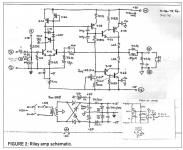
the basic circuit is attached. Let me know what you think,
Jan
But did you know that they also developed a power amp for use in their own active speakers?
I recently again read my interview with Siegfried and thought that the design, shown and discussed in the interview, might be of interest to builders here.
It has several unusual features that you could explore.
The full interview is at https://linearaudio.nl/sites/linear.../siegfried_linkwitz_audioxpress_interview.pdf ;
the basic circuit is attached. Let me know what you think,
Jan
Attachments
Let me know what you think
Hi, Jan!
Main questions:
1. Why no CCC as the IPS tail current source (pic 1). This compromises CMRR and moreover allows common mode error to be converted to differential mode.
2. Too much dominant pole capacitor (pic 2). This will compromise high-frequency distortion due to lack of feedback depth at higher side of audioband. Such a capacitor can be easily divided to two with thirdh-fourth in capacitance and a something 1-2k resistance to ground. This will provide an amp with second order compensation and keep at least 20-40 dB feedback depth at 20 kHz.
3. Relatively bad coupling between first IPS stage and second VAS stage (also pic 2). IPS loaded to a simple current mirror have high output resistance and being loaded straightly to a VAS transistor it have relatively high load. This will really drop feedback depth and compromise performance.
4. Compound Feedback pair aka Sziklai transistor (pic 3) not a best choice to couple with simple VAS and not a good choise as output stage. First it have relatively small current gain compared to EF3 and due to this it hugely load VAS high output impedance point. This again drops feedback depth and THD figures. Second it have huge crossover effects because at high-power output transistor switch-off it couples load to VAS through just one medium powered transistor with a current gain of a order of ~100-150 times. Again feedback depth drop and THD rise.
5. Overall noninverting config. Too bad to be true.
Conclusion.
Is this a joke, Jan?


Hi, Jan!
Main questions:
1. Why no CCC as the IPS tail current source (pic 1).
Note the date on the schematic. 1974. Pretty sure people didn't bother with CCS in discrete amps back then and was still considered a trick for the IC designers who pretty much HAD to do it.
So you didn't read the article where this came from?
Jan
So you didn't read the article where this came from?
Heh, Jan, you have asked what we think about schematic, not from where it came.
I was unable to find design goals/principles in the article so i just pointed to a most known issues.
Interview pdf p. 1, third column - are you sure about the spelling of "Filbertz Transformer" ?
I count on you as my proofreader!
Jan
The full interview is at https://linearaudio.nl/sites/linear.../siegfried_linkwitz_audioxpress_interview.pdf ;
Thanks for posting the interview. This was a trip down memory lane back to very exciting times. SL and KEF were hugely influential for me (and others, no doubt) getting seriously into speaker system design.
Using a zener reference and a resistor to define the LTP current is surprisingly good (I simmed it a few years ago), so IMV quite ok.
Why use a current source for the VAS load? To increase the open loop gain - so again, a pretty good use of resources given the vintage.
Its easy to forget just how expensive semiconductors were in 1974 - I remember when a BC109 cost a hobbyist 40c and a 741 3~4x that.
re the 2 pole compensation, Robert Dobkin had published about this (re the LM301 opamp IIRC) only a few years earlier - this type of comp wasn't mainstream in audio in 1974. Besides, with all that Matti Otala stuff about to hit the fan I would imagine there would have been a lot of flack about that 😉
Neat circuit - thanks for posting Jan.
(Might be an idea for a member to sim this in LTspice - I'd volunteer but too busy at the minute.)
Last edited:
3. Relatively bad coupling between first IPS stage and second VAS stage (also pic 2). IPS loaded to a simple current mirror have high output resistance and being loaded straightly to a VAS transistor it have relatively high load. This will really drop feedback depth and compromise performance.
My understanding (please correct me if I'm wrong) is the IPS acts as a transconductance stage, and the overall gain is IPS gm times VAS transimpedance. Therefore, voltage gain of the IPS is irrelevant. Due to shunt feedback, the input to the VAS is a virtual ground (in fact, this is a stated assumption of the math derivation of TPC) and all the current swing from the IPS flows into the VAS. Low input impedance here is an advantage, then.
The purpose of adding the beta-enhancement transistor to the VAS is not to raise the load impedance seen by the IPS, but to increase the local loop gain around the VAS, and to greatly reduce the required current from the IPS.
Bottom line, as I understand it, is you want the input to the VAS to look like a short circuit. I am frequently wrong, and eager to shed misconceptions, but this makes sense to me.
Yes the VAS (more correctly 'transimpedance stage or TIS) is an integrator so you want high loop gain around it and that's what the helper transistor does in combination with the main VAS transistor.
See Bruno Putzeys 'The F Word' for a full dissection.
See Bruno Putzeys 'The F Word' for a full dissection.
I count on you as my proofreader!
Jan
Re "Filbertz Transformer" it should be Philberth and deserves a dedicated thread.
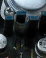
What I also found interesting is that they apparently found a bias method to avoid adjustment. Although you'd have to select a FET and have a really good thermal compensation loop.
The article also has a pic of a built-up PCB, and the heatsinks are small compared to the monsters we use these days. OTOH, this is for active speakers, not for 1 hr full power on a workbench 😎
If you look carefully, you see the bias FET connected to the heatsink finger with a small plastic tube.
And putting those fuses inside the loop - brilliant!
Jan
Attachments
Last edited:
Yes - the value of R6 is quite critical. The value I have shown is far too low so the OPS current is too high. You need about 220-250 Ohms to set the VAS curren tto c. 4-5mA for 90mA OPS bias current.
Anyway, I'll leave it for others to play with.
Anyway, I'll leave it for others to play with.
The purpose of adding the beta-enhancement transistor to the VAS is not to raise the load impedance seen by the IPS, but to increase the local loop gain around the VAS, and to greatly reduce the required current from the IPS.
Hmm. Ok.
We add a follower, but it increase gain. Not bad. Give me two, please.
Let's talk about in terms of impedance coupling and stage loading.
Just imagine current consumption from IPS in those different cases. VAS as integrator have huge gain, but frequency dependant input impedance. Beta-enhancement transistor just converts high output impedance of the IPS to the lower input impedance of the VAS. In the absense of those beta-enhancement transistor IPS output current just flows to the lowish VAS input impedance providing literally no gain.
Now with it in place amp like to have two gm stages (IPS loaded to a mirror and VAS loaded to a current source) and two high-impedance points - IPS output (having small swing) and VAS output (having huge swing), so up to ~120 dB overall gain through audioband with easy.
Now you must cope such a Niagara of gain.
.jpg")
.jpg")
And putting those fuses inside the loop - brilliant!
Jan
When one of those fuses fails and the other doesn't, a massive DC voltage would then be applied to your speaker, almost certainly causing a fire. Decidedly not my cup of tea.
That is no different when one fuse blows with fuses in the + and - supply line.
But as long as the fuses are OK (which is normal situation), they have much less impact on the sound quality.
Jan
But as long as the fuses are OK (which is normal situation), they have much less impact on the sound quality.
Jan
That is no different when one fuse blows with fuses in the + and - supply line.
But that amplifier has no DC fault protection, and, in any case, it is far better to have the fuses in the supply rails where the distortion they generate will not be an issue.
- Home
- Amplifiers
- Solid State
- Linkwitz-Riley POWER AMP