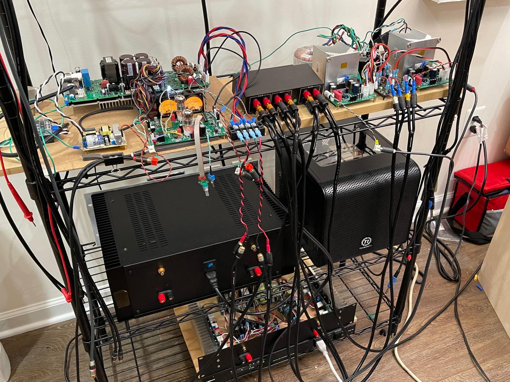
I really like your amp chassis.
Another way to layout the amp would be to place both amp boards on one heat sink. Then you could mount the trafo vertical at the back corner with the power supply on the same side as the trafo. I try to keep the AC connections short and as far from the amp boards as room allows. My heat sinks are tiny compared to your heat sinks and they barely get warm, but maybe I don't push the amp too hard.
Another way to layout the amp would be to place both amp boards on one heat sink. Then you could mount the trafo vertical at the back corner with the power supply on the same side as the trafo. I try to keep the AC connections short and as far from the amp boards as room allows. My heat sinks are tiny compared to your heat sinks and they barely get warm, but maybe I don't push the amp too hard.
I would move the power trafo away by mounting it on its side using a L bracket.
Then you could mount the trafo vertical at the back corner
Transformer is just a hair wider than the case is tall, so I cannot side mount it.
Good idea though, would have freed up a bunch of space...
David.
Any other comments about the layout?
Using the horizontal mounting version of the TDA7293 and mounting the PCBs vertically on the heatsinks will free up lots of space.

TDA7293HS STMicroelectronics - Amplifiers - Audio - Distributors, Price Comparison, and Datasheets | Octopart component search
Also, if the chassis height permits, you could also mount the protection PCB vertically on the rear panel and/or stack the PS board above the toroid.
I don't have a lot of amp building experience, how hot will the TDA7293's get?
Can I stack the two amp boards?


This configuration with the stacked boards really simplifies the signal path as well.
Can I stack the two amp boards?
This configuration with the stacked boards really simplifies the signal path as well.
I don't have a lot of amp building experience, how hot will the TDA7293's get?
...
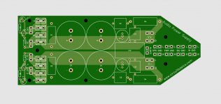
The board on the top/right side looks like a protection for speakers with two relays (difficult to read what is written). Very simple. Is it?
The board on the top/right side looks like a protection for speakers with two relays (difficult to read what is written). Very simple. Is it?
It is the UPC1237 speaker protect board from buildaudioamps.com,
*** Click here to go to Build Audio Amps speaker protect board ***
I redrew the circuit in Sprint and had some boards made.

There is also a speaker delay/protection circuit available here on the DIYAudio store ( Soft Start & Speaker Turn-On Delay / DC Protector Combo – diyAudio Store ) but you have to buy the set of two boards: softstart & speaker protect/delay.
The Xmas amp moved up one level higher in the amp rack. I’m listening to it almost everyday now. Still loving the sound of this amp. So pleasant and dynamic - no fatigue at all. Can listen all day.
Top row: prototype for Emerald Physics under development (600.2SE) using IcePower 1200AS2 module with HyperSET SS/tube buffer preamp, Xmas amp; middle row: Alpha Nirvana 40w Class A amp by Hugh Dean, Aspen Amplifiers (Hugh Dean) Glass Harmony (1 channel) 50w SE Class A amp; bottom row is VHEX+ amp 100w Class AB by Vzaichenko.
Top row: prototype for Emerald Physics under development (600.2SE) using IcePower 1200AS2 module with HyperSET SS/tube buffer preamp, Xmas amp; middle row: Alpha Nirvana 40w Class A amp by Hugh Dean, Aspen Amplifiers (Hugh Dean) Glass Harmony (1 channel) 50w SE Class A amp; bottom row is VHEX+ amp 100w Class AB by Vzaichenko.
Last edited:
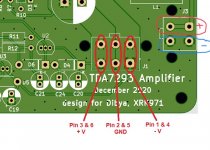
Can someone confirm I have the all my polarities correct before I start connecting wires?

Thank you,
David.
Thank you,
David.
Last edited:
I can’t claim the original photo (maybe X?) but I added in the speaker outputs.
The square pad on J2 connects with C101 so it’s the “+” input signal. See Post #186 for correct schematic.
Cheers, Pete
The square pad on J2 connects with C101 so it’s the “+” input signal. See Post #186 for correct schematic.
Cheers, Pete
Attachments
Last edited:

I can’t claim the original photo (maybe X?) but I added in the speaker outputs.
The square pad on J2 connects with C101 so it’s the “+” input signal. See Post #186 for correct schematic.
Cheers, Pete
Original image credit goes to twocents….
See posts #691-695
Last edited:
WAIT WAIT WAIT!!! I blew up my TDA chips because of incorrect polarity.
Yes, that was my image - but I am NOT convinced that it is correct. I think DaveFred's image in Post #731 is correct.
If you look at the three connections, it looks like the square pads are always the + polarity. Therefore the power input should be - / Gnd / + from left to right on the board (square pad is on the right), like DaveFred has it in Post #731.
Can someone please confirm that this convention (square pad = +) is always applied and on this board too?
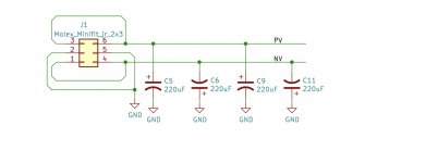
C9 is pos rail, C11 is neg rail. Board seems a little tricky to read but the schematic is clear as a bell.!
Very confusing statement 😕C9 is pos rail, C11 is neg rail.
Yes, schematic is clear and shows pin numbers for the Molex connections, but how do they translate to the board?Board seems a little tricky to read but the schematic is clear as a bell.!
What JimK04 states is that the molex pin connected to C9 is the positive rail so a continuity check with a meter from the left pin of the molex to the negative pad on C9 will reveal the positive power in location. If you look at my amp images blown up you can just see a little + sign above the left pin.
Attachments
Very confusing statement 😕
Yes, schematic is clear and shows pin numbers for the Molex connections, but how do they translate to the board?
All the confusion lies with the square solder pads. I believe their only significance is to reference the start of the sequence , as in, Pin#1 or Connection #1. They don’t represent polarity. So the molex position #1 (see the attached pic from the amp schematic ) and position #4 lead to the “-“ side of one set of capacitors while positions 3&6 lead to the “+” side of the other caps.
The pic in #732 is correct
Attachments
Last edited:
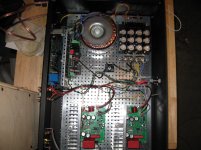
Just to reiterate signal lost’s pic here are pics of my PS board (output + rails on top & - rails on bottom) which in the other pic are represented by colored wires (yellow is “-“ rail, black is “+” rail and white is ground).
Attachments

- Home
- Amplifiers
- Chip Amps
- Xmas Amp - Dibya's TDA7293 by Jhofland