I'm looking BACK now on the Wolverine.
It's easy now , after the spook.
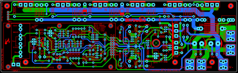
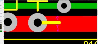
(below) I pushed your inner IPS routing further.
- R15 short ground route
- R6,7,8 pushed down ... your (top) blue trace lined up with all the others.
-R21 pushed up , lines up with 6,7,8.
Main ground and VAS drive have lots of room now.
If you get to the Spook , you will see why this one is cake now.
I was changing sides all night on the spook traces.
PS - R17 and R15 can run the same trace. NO return currents to really worry about.
Nothing will get modulated on that trace.
OS
Hi OS,
Thanks for taking a closer look.
Can you modify my V1.5.5 file and sent it back to me or do you want me to modify mine based on your image and comments?
I am just about finished checking the IPS.
Last edited:
Your file was like a Macro. I could dissolve the components from the traces ,
but the traces were one.
Go ahead , make the changes but leave the layout workable.
OS
but the traces were one.
Go ahead , make the changes but leave the layout workable.
OS
Your file was like a Macro. I could dissolve the components from the traces ,
but the traces were one.
Go ahead , make the changes but leave the layout workable.
OS
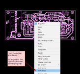
I just grouped the IPS section.
To un-group it. Just right click and and select split group
I fix it based on your image and notes no worries. 🙂
Attachments
Last edited:
VAS - Check and Tweaked. IPS updates made.
Hi OS.
I have finished now with the checking of the VAS and I have made those changes you suggested to the IPS. I also made you a short YouTube video which you maybe interested in watching with some more sprint layout tips.
Sprint Layout Tips - YouTube
I hope to continue soon with finishing off the OPS.
Thanks for your support. We are all doing a great job to make this
an Awesome Amplifier. I am so looking forward to building it
and taking some measurements.
Attachments
Hi OS,
Stuart and I were looking at your wonderful PCB. We also discussing components and lead spacing.
What type of caps have you got in mind for C4a, C4b, C110 and C111?
The reason I'm asking is that Mica caps from Mouser have a lead spacing of 5.9mm.
Stuart and I were looking at your wonderful PCB. We also discussing components and lead spacing.
What type of caps have you got in mind for C4a, C4b, C110 and C111?
The reason I'm asking is that Mica caps from Mouser have a lead spacing of 5.9mm.
Correction to my post above I have found mica caps (CDA15ED) from Mouser that are 5.1mm lead spacing.
Hi OS,
Stuart and I were looking at your wonderful PCB. We also discussing components and lead spacing.
What type of caps have you got in mind for C4a, C4b, C110 and C111?
The reason I'm asking is that Mica caps from Mouser have a lead spacing of 5.9mm.
For C4a, and C4b capacitors I would try Amtrans AMCH PP caps. They are very good sounding, and not too expensive.
Hi OS,
I think, I'm done.
I'm happy to make any other changes or addition that you or other members find and you wish me to add.
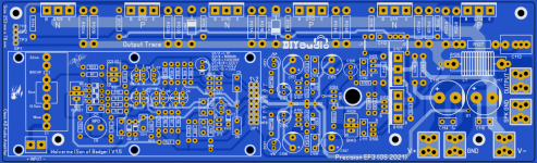
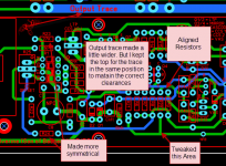
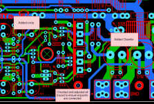
Updates noted in images.
IPS, VAS & OPS are all checked.
I think, I'm done.
I'm happy to make any other changes or addition that you or other members find and you wish me to add.
Updates noted in images.
IPS, VAS & OPS are all checked.
Attachments
Last edited:
Hi Stuart!
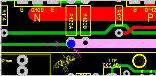
I recommend to add small series resistors, say 10-22ohms, with the testpoint outputs. It protects the transistors, against any short circuit during measurement.
Sajti
I recommend to add small series resistors, say 10-22ohms, with the testpoint outputs. It protects the transistors, against any short circuit during measurement.
Sajti
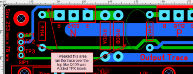
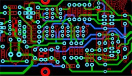
Stuart looks really nice about values don't add the values leave it as it is example R1, C1, D1, etc is fine, the size PCB I would place that under the PCB as copper letter so to avoid having too much letters on the PCB on top, this emitter resistor pads and diode D103,104 can be align with the output trace here,
note:
🙂 Ostripper probably thinking this maniacs locos hahahahaha I love this 😀
regards
Juan
note:
🙂 Ostripper probably thinking this maniacs locos hahahahaha I love this 😀
regards
Juan
Attachments

Stuart looks really nice about values don't add the values leave it as it is example R1, C1, D1, etc is fine, the size PCB I would place that under the PCB as copper letter so to avoid having too much letters on the PCB on top, this emitter resistor pads and diode D103,104 can be align with the output trace here,
note:
🙂 Ostripper probably thinking this maniacs locos hahahahaha I love this 😀
regards
Juan
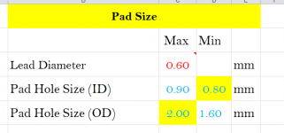
Thanks Juan for taking a look but for those traces we need to make an exception. If we move the trace to the center it will become to close to the other pads on R117, R115, R118, R116, R119
I just did notice something the Pads are are a bit larger that I would usually use for 1/4 watt and 1/2 watt resistors they are 1mm drill size with a OD of 2.4mm.
I normally use 0.9mm x 2.0mm for a 0.6mm lead.
What do you guy's think?
Attachments
Hi Stuart!
I recommend to add small series resistors, say 10-22ohms, with the testpoint outputs. It protects the transistors, against any short circuit during measurement.
Sajti
We can probably fit that in. Lets see what OS thinks.
I usually use Digikey 36-5125-ND Test points then you can space
them further apart. I could put them at 5mm apart so there
would be less change of a short.
Hi Stuart!
I recommend to add small series resistors, say 10-22ohms, with the testpoint outputs. It protects the transistors, against any short circuit during measurement.
Sajti
Those aren't test points. They're connections for an external protection system.
Those aren't test points. They're connections for an external protection system.
Sorry, the TP name was misleading.
Thanks Juan for taking a look but for those traces we need to make an exception. If we move the trace to the center it will become to close to the other pads on R117, R115, R118, R116, R119
I just did notice something the Pads are are a bit larger that I would usually use for 1/4 watt and 1/2 watt resistors they are 1mm drill size with a OD of 2.4mm.
I normally use 0.9mm x 2.0mm for a 0.6mm lead.
What do you guy's think?
hi ST I just send the files to you I kept the one you did and I made one with the changes, now I know that the SIP1 is not for bias reading but for protection thanks jwilhelm 🙂
Last edited:
Hi OS,
I think, I'm done.
I'm happy to make any other changes or addition that you or other members find and you wish me to add.
Updates noted in images.
IPS, VAS & OPS are all checked.
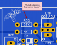
Attachments 1,3,4 are good , add the values if you want.
#2 is the issue.
(below is ideal)
Let me explain , R20/21 are fed by a possible 120V p-p signal.
This is why the NFB trace is far away from others.
R20 is the critical TMC feedback , fed with 120V ... needs to be so
close to C4a/b. I swapped R19 and 20 , you see.
VAS stuff should stay in their own area.
R21 is main NFB , also fed with a 120V signal . it is also distanced from
the very high Z R6/7/8 (and lifted ground) ..
Copy my changes exactly.
PS - please make your IPS workable , it renders as one big macro.
Edit - consider the whole VAS as a (dangerous) IEC "keepaway" zone 120-130V.
OS
Attachments
Last edited:
Stuart looks really nice about values don't add the values leave it as it is example R1, C1, D1, etc is fine, the size PCB I would place that under the PCB as copper letter so to avoid having too much letters on the PCB on top, this emitter resistor pads and diode D103,104 can be align with the output trace here,
note:
🙂 Ostripper probably thinking this maniacs locos hahahahaha I love this 😀
regards
Juan
Its good having 2 more layout "fanatics" to help with the "headache".😀
O
Copy my changes exactly.
PS - please make your IPS workable , it renders as one big macro.
Will do... thanks for your feedback.
Did you read my post #503 and watch my YouTube video from post #504?
Stuart , I am not pulling this stuff "out of a hat".
For example , the tip to just use the same ground return for R15/17 is based
on the fact that the two resistors that are at 1mA are in phase and modulate at 20uA.
That trace need to be nothing but a good (G2) ground.(below)
A cap multiplier or my Spooky regulators need to at least be tapped in the middle (or starred) as they could return many mA's under high load/ripple.
The regs less so , since they are already filtered initially by the multipliers.
OS
Attachments
- Home
- Amplifiers
- Solid State
- DIYA store "Wolverine" (Son of Badger) .... suggestions ??