Gentlemen,
I am a valve guy, my knowledge about transistor circuits is rather meagre. So I would like to ask for some help to "translate" the functionality of the tubed HV differential booster stage shown below to silicon.
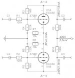
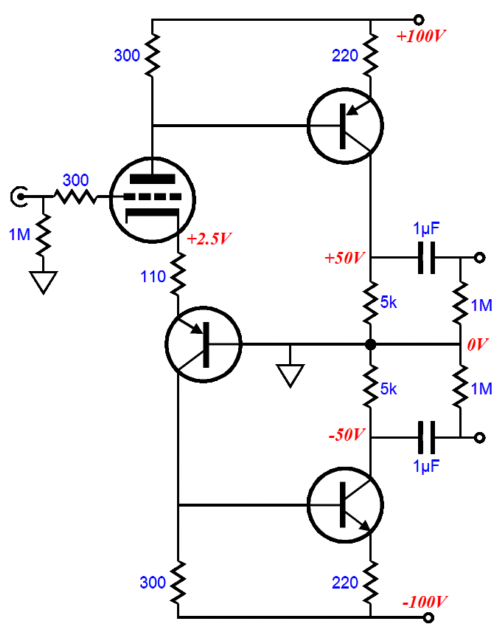
Given its simplicity and low current consumption this stage works surprisingly well. It shows wide swing- and drive capabilities and rather lowish distortion. It consists of two anode / plate followers with a common unbypassed cathode resistor. The plate followers trade gain for low Zout and low(er) distortion. The unbypassed common cathode resistor may help a little bit further to linearize the tubes transfer function especially with wide anode swings.
I suspect translating this booster stage concept to sand state would give some benefits; my primary intention would be getting a wider output swing possible for the same (or less) supply voltage.
I already googled for BJT based "collector follerwers" but soon got stuck. As I understand the circuits I found seem to point more toward providing the biasing for the transistor considering its base current (which is almost absent with tubes) and also to provide DC feedback for operation point stabilization.
Looking for MOSFET "drain followers" I found even less information, but because of their very high input impedance they seem to be a more "natural" choice to translate that circuit to silicium. On the other hand such MOSFETs show much more input capacitance than tubes - but required stage gain is lowish and so will be expected Miller C.
With these considerations I would just go the MOSFET path for the translation.
Or are there any other concepts for a "simple" solid state HV diff boost stage you would suggest to have a look at?
Thank you very much and kind regards, Tom
I am a valve guy, my knowledge about transistor circuits is rather meagre. So I would like to ask for some help to "translate" the functionality of the tubed HV differential booster stage shown below to silicon.
Given its simplicity and low current consumption this stage works surprisingly well. It shows wide swing- and drive capabilities and rather lowish distortion. It consists of two anode / plate followers with a common unbypassed cathode resistor. The plate followers trade gain for low Zout and low(er) distortion. The unbypassed common cathode resistor may help a little bit further to linearize the tubes transfer function especially with wide anode swings.
I suspect translating this booster stage concept to sand state would give some benefits; my primary intention would be getting a wider output swing possible for the same (or less) supply voltage.
I already googled for BJT based "collector follerwers" but soon got stuck. As I understand the circuits I found seem to point more toward providing the biasing for the transistor considering its base current (which is almost absent with tubes) and also to provide DC feedback for operation point stabilization.
Looking for MOSFET "drain followers" I found even less information, but because of their very high input impedance they seem to be a more "natural" choice to translate that circuit to silicium. On the other hand such MOSFETs show much more input capacitance than tubes - but required stage gain is lowish and so will be expected Miller C.
With these considerations I would just go the MOSFET path for the translation.
Or are there any other concepts for a "simple" solid state HV diff boost stage you would suggest to have a look at?
Thank you very much and kind regards, Tom
Attachments
You can pretty much replace the triodes in the circuit with high voltage depletion MOSFET. LND150 is rated at 500V. You may need to parallel LND150. It should drop straight into your valve circuit. The cathode resistors, now the source resistors will need adjustment to get the drain operating point (formerly the anode) to the desired value.
One issue is power dissipation. The T092 package is rated at 0.74W max. Two in parallel should work and might need a small heat sink. The paralleled devices will increase the input capacitance so check datasheet for compatibility. The TO243 surface mount package would work as a single but would need PCB copper area as heat sink. This would keep the input capacitance to around 7.5pF.
The point to note is that the depletion MOSFET is similar to a triode in that the source is positive relative the gate. The voltage has a production spread. Expect about 1V compared to 0.8V. As they draw more current, the gate-source voltage will reduce and the devices can even operate with gate positive with respect to the source. They are not as robust as valves so avoid wild resistor value changes. Make a low voltage circuit to match the FETs if choosing T092.
An externally hosted image should be here but it was not working when we last tested it.
An externally hosted image should be here but it was not working when we last tested it.
Last edited:
Gentlemen,
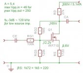
thank you for your input! For a "translation" into solid state, I decided to keep closer to the original. Using an IRF710 MOSFET which measured Rgs,on = 3,6V for 5mA, I recomputed one half of the diff booster for 300V supply voltage and measured the results of this "drain follower", see schematic attached. The results are pretty encouraging; very wide output swing with quite low distortion (at least for a simple valve substitute).
Only step left is to double the circuit using a common drain resistor with half the resistance, which is trivial. I´ll post the final result somewhen this week.
One question remains, though: How to compute the exact input impedance of this "drain follower" circuit?
Thank you and kind regards,
Tom
Attachments
Last edited:
The problem is not with the resistance, but with the gate nonlinear capacitance of 170 pF or more. With a 100 kΩ resistor, you get a low cutoff frequency. If you reduce the resistor, the source will operate on a capacitive load. Gate-drain voltage + -20V.
Additional transistors will be required.
The complete analogy doesn't work.
Additional transistors will be required.
The complete analogy doesn't work.
Last edited:
Hello OldDIY,
As noted in the schematic, I measured fu,-3db to be about 120 kHz with a low generator impedance, which is fine for my purpose. Sure there is visible slewing on the rising edges when using a 10 kHz square wave input signal, but I´ve seen much worse in tube audio circuitry using a whimpy driver working into the Miller C of the following stage.
Miller C loads of 100 pF and even considerably more are quite common when driving triodes or triode strapped pentodes.
But you are right of course that this won´t be a one-to-one drop in replacement, since the original tubed stage shows a much lower input capacitance, which is easier to drive, indeed.
Anyway, for now I´ll proceed with a complete diff booster based on this stage and do some more measurements.
Thank you again!
Tom
With a 100 kΩ resistor, you get a low cutoff frequency.
As noted in the schematic, I measured fu,-3db to be about 120 kHz with a low generator impedance, which is fine for my purpose. Sure there is visible slewing on the rising edges when using a 10 kHz square wave input signal, but I´ve seen much worse in tube audio circuitry using a whimpy driver working into the Miller C of the following stage.
Miller C loads of 100 pF and even considerably more are quite common when driving triodes or triode strapped pentodes.
But you are right of course that this won´t be a one-to-one drop in replacement, since the original tubed stage shows a much lower input capacitance, which is easier to drive, indeed.
Anyway, for now I´ll proceed with a complete diff booster based on this stage and do some more measurements.
Thank you again!
Tom
Last edited:
The plate followers trade gain for low Zout and low(er) distortion
I already googled for BJT based "collector follerwers" but soon got stuck.
No such circuits, there are cathode-followers, source-followers and emitter-followers, but none apply here.Looking for MOSFET "drain followers" I found even less information,
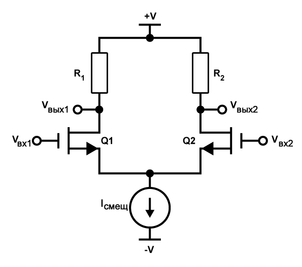
You have an AC-coupled differential pair with local feedback, which may be class A or AB or B, its hard to tell from the circuit,
suspect its class A as its small signal stuff.
The equivalent transistor circuit would probably be a long-tailed pair rather than the separate circuits here.
Last edited:
Hi Mark,
Excuse me that i am an old fashioned tube guy and also tend to refer to old terminology. In the case of the first circuit shown it really can be split in two anode- or plate followers with a common cathode resistor. Not knowing better, I just made the "mistake" of mapping the names of the valve electrodes to their corresponding names when using BJTs and FETs, didn´t I?
If you don´t know what a plate follower and the math behind it is please have a look at this article from C. Boegli, 1960: https://www.aikenamps.com/images/Documents/anode.pdf, which likely preceedes all literature regarding "similarly" working circuits using BJTs and FETs.
Kind regards, Tom
No such circuits, there are cathode-followers, source-followers and emitter-followers,...
Excuse me that i am an old fashioned tube guy and also tend to refer to old terminology. In the case of the first circuit shown it really can be split in two anode- or plate followers with a common cathode resistor. Not knowing better, I just made the "mistake" of mapping the names of the valve electrodes to their corresponding names when using BJTs and FETs, didn´t I?
If you don´t know what a plate follower and the math behind it is please have a look at this article from C. Boegli, 1960: https://www.aikenamps.com/images/Documents/anode.pdf, which likely preceedes all literature regarding "similarly" working circuits using BJTs and FETs.
Kind regards, Tom
Last edited:
> If you don´t know what a plate follower and the math behind it is
More people should know that.
However I doubt this is the path you want for a differential amplifier. The two sides will fight each other.
More people should know that.
However I doubt this is the path you want for a differential amplifier. The two sides will fight each other.
https://inst.eecs.berkeley.edu/~ee105/fa03/handouts/lectures/Lecture17.pdf
https://www.electronics-tutorials.ws/amplifier/amp_2.html
https://www.electronics-tutorials.ws/amplifier/amp_2.html
An externally hosted image should be here but it was not working when we last tested it.
Last edited:
Hi OldDIY,
I think that´s a different thing you are pointing at - this is just partly "fixed" biasing of a BJT, maybe including an elevated emitter.
Please note that there is a FB path from the anode to the grid in the original circuit (or from the drain to the gate in the "translated" circuit). This is not the case with the circuit you show.
Kind regards, Tom
Last edited:
An externally hosted image should be here but it was not working when we last tested it.
https://www.electronics-tutorials.ws/amplifier/mosfet-amplifier.html

Field-Effect Transistors (AC Analysis) - Equations Library | CircuitBread
These are the basic circuits for switching on transistors.
The inclusion of a resistor in the emitter (source) means NFB.
Including a resistor between the base (gate) and the collector (drain) is also a form of NFB.
Last edited:
Your schema # 1 given # 6 is converted to # 10.
It may be necessary to match a pair of identical mosfets and add balancing circuits.
It may be necessary to match a pair of identical mosfets and add balancing circuits.
Last edited:
Suspect Mr Boegli might have gone on a tangent that turned out to be a dead end, evolution-wise. I've certainly never heard of a 'plate follower'.
Just me, though ..
The circuit you're working on will work. Slightly better linearity and DC stability could probably be had with a Depletion-Mode MOSFET choice, though.
Cheers
edit: Oops, forgot to mention -- you'll probably have to reduce the 100k in series at the input.
Just me, though ..
The circuit you're working on will work. Slightly better linearity and DC stability could probably be had with a Depletion-Mode MOSFET choice, though.
Cheers
edit: Oops, forgot to mention -- you'll probably have to reduce the 100k in series at the input.
Last edited:
- Home
- Amplifiers
- Solid State
- HV diff booster stage - please help / suggest