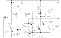
I found a schematic for a LM833 on the data sheet and I labeled all the components. I have been looking for the schematic of an op-amp to try to build out of discrete transistors to see how that works, especially because it might be useful to try to build it from 2N5551/2N5401 to increase the voltage range of the amplifier. I would have to decrease the quiescent currents so this might reduce the slew rate however, but it might still be interesting to try.
First of all, does this look like a good design to start with? I looked at the NE5532 schematic but it required multiple emitter and multiple collector transistors which I think are going to be hard to get, or match parts to provide work-alikes.
Is the P MOSFET or P JFET (Q2) I think is there to ensure that Q1 turns on when the chip is powered on?
It looks like C2 is a compensation capacitor for unity gain stability perhaps?
Is it possible to get performance from a discrete design that is comparable to the IC version, or are the matched components in the manufactured chip required to get low values of offset and distortion?
Attachments
you need to do tons of simulations before even have a functional model then it will never have similar thermal stability to the IC as prototyping for discrete world is an entirely different game than IC...
What are those resistor values?
Are there any key "matching" requirements? (Yes, a diode vs a transistor, which is hard in discrete work.)
In general, monolithic design is very different. Take a discrete "power amplifier" and design-off the last stage. Yes, Self and Cordell become your best friends.
Are there any key "matching" requirements? (Yes, a diode vs a transistor, which is hard in discrete work.)
In general, monolithic design is very different. Take a discrete "power amplifier" and design-off the last stage. Yes, Self and Cordell become your best friends.
Is it possible to get performance from a discrete design that is comparable to the IC version, or are
the matched components in the manufactured chip required to get low values of offset and distortion?
Very difficult, since monolithic ICs use matching, laser trimming, and tracking,
where discrete designs cannot.
One thing I was trying to figure out is why someone would use something like the Burson Discrete Op-Amp:
Supreme Sound Opamp V4 – Burson Audio
I don't really buy their largely unsupported argument that IC op-amps are somehow inferior. I do however think that they can probably get it to work ok enough, and they claim to match resistor values and there is some trimmer on there that must be used to perhaps null the input offset.
My reasoning was that perhaps one could make a high-voltage op-amp which might be useful as a component for a power amplifier, or for laboratory use, for example amplifying high voltage signals to drive piezos. I have read Self and Cordell's books on power amplifier construction and can probably piece something together from that.
If you've designed your own discrete opamps from scratch, built them on PCBoards, debugged and stabilized them, and then made measurements ...
then I think you won't have an awful miserable time copying the LM833 in discretes. The job isn't difficult if the worker is expert.
then I think you won't have an awful miserable time copying the LM833 in discretes. The job isn't difficult if the worker is expert.
First of all, does this look like a good design to start with?
No. Clearly no.
Very difficult, since monolithic ICs use matching, laser trimming, and tracking, where discrete designs cannot.
Even more.
Monolitic crystal have no relatively huge PCB parasitics - first of capacitance and leaks.
So any of the discrete design can't use IC schematic and compensation straightly.
The discrete Jensen 990 has been robustly documented and can be built of jellybean parts or exotic parts as you wish.
Opamps of ANY voltage are readily bought or designed. Often a true "opamp" is not essential. I once slapped-up a diff-in diff-out 300V "opamp". Worked great.
Opamps of ANY voltage are readily bought or designed. Often a true "opamp" is not essential. I once slapped-up a diff-in diff-out 300V "opamp". Worked great.
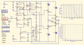
Using Qucs-S, which is a graphical spice simulation program, I threw together a simple op-amp based on a power amp design I made.
I have not really tested it very thoroughly yet since I just made it, but in the noninverting configuration there is definitely a significant DC offset when there is a significant impedance to the signal source. The original amplifier I cribbed part of this from, however, uses a capacitor in the feedback to remove the DC offset.
However, the distortion seems to fairly low at 20 kHz with +/-80 volts of swing, about 0.1%.
I'm sure that other stuff like CMRR and PSRR are not that great, but it's a start.
How would a IC op-amp design differ from a poweramp design, especially given that IC op-amps are used in power amplifiers to linearize them?
Attachments
The first difference would be the open loop gain which in a power amp is usually 10...1000 times smaller than the open loop gain of an op-amp...Compensations become less critical in a power amp...Try make a power amp stable in unity gain!...
The discrete Jensen 990 has been robustly documented and can be built of jellybean parts or exotic parts as you wish.
Took me a few pcb iterations to get that one stable... Used it as a headphone driver for som time.
Problem with discrete designs of monolithic circuits is that you don't get the thermal uniformity amongst the components that the monolithic approach offers.
Ok, here's the current state of things (maybe progress?)
I have limited quiescent currents to around 1 mA so that with +/- 100 V the transistors dissipate 100 mW (2N5401/2N5551 has 500 mW maximum dissipation). I included the DC bias points to show that.
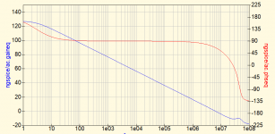
The open loop gain at 1 Hz is 125 dB rolling off at -20 dB/dec and the phase margin is about 60 degrees, and the gain margin about 7 or 8 dB.
It seems to be unity gain stable, for example I am driving it with a +/- 80 V sine wave with unity gain. The distortion seems to be < 0.005% at 80 kHz.
So either I am doing something very right, or very wrong...
I have limited quiescent currents to around 1 mA so that with +/- 100 V the transistors dissipate 100 mW (2N5401/2N5551 has 500 mW maximum dissipation). I included the DC bias points to show that.
The open loop gain at 1 Hz is 125 dB rolling off at -20 dB/dec and the phase margin is about 60 degrees, and the gain margin about 7 or 8 dB.
It seems to be unity gain stable, for example I am driving it with a +/- 80 V sine wave with unity gain. The distortion seems to be < 0.005% at 80 kHz.
So either I am doing something very right, or very wrong...
Attachments
Trying to build a precision DC opamp from discrete parts would be much harder than for audio - the thermal drift in the input section would likely be horrendous compared to on-chip inter-digitated transistors used in precision opamps - but thermal drift is inaudible as its subsonic, so is almost of no consequence for audio.
And some integrated opamps are both excellent at DC and audio performance simultaneously, and even though expensive, are usually considerably cheaper than a discrete opamp - bit of a no-brainer to me.
As for the discrete LM833 circuit in this thread I'd suggest adding back-to-back diodes across the inputs to prevent noise-performance degradation, just like the original - if you want the noise performance to last its best to protect the input transistors from overload.
....I have limited quiescent currents to around 1 mA so that with +/- 100 V the transistors dissipate 100 mW (2N5401/2N5551 has 500 mW maximum dissipation). I included the DC bias points to show that.
The open loop gain at 1 Hz is 125 dB rolling off at -20 dB/dec and the phase margin is about 60 degrees, and the gain margin about 7 or 8 dB.
It seems to be unity gain stable, for example I am driving it with a +/- 80 V sine wave with unity gain. The distortion seems to be < 0.005% at 80 kHz.
So either I am doing something very right, or very wrong...
I assume this is just a simulation? Spice models are only an approximation of reality and often don't include all the parameters and variables one would actually encounter in the finished product.
Why is such a high voltage needed?
Are you using the minimum Beta of 50 for the BJTs (lower process specification) or the max beta of 250 (upper process specification) on the transistors? On real transistors, the beta tends to inversely track the VA (Early voltage) also tracks Bv. The Spice model normally has just a single Beta, VA & Is (Vbe), unless you are using some corner models or statistical models.
The SPICE model may not properly predict the quasi-saturation of the BJT at low Vce, so one may need to check it on a curve tracer to verify for the specific operating conditions.
Try the simulation with real world Vbe mismatch of 10mV to 30mV, by insertion of simulation voltage offsets (unless you are going to manually match & select the transistors) and temperature differences between transistors of 5-10 C (unless you are using thermal coupled pairs & iso-thermal mounting of the input vs output devices). How are you going to make bias string diodes match the output transistors ...thermal coupled and trimmed? When the output signal swings, the power dissipation will heat up the output transistors and change the Vbe.
You could also try a Monte Carlo simulation with variation of temperature between devices (dT), variation in Vbe (Is), variation in BJT Betas, ect...
You will probably need to trim Vos on the input differential pair and the bias collector current on the class AB output, even if the thermal coupling is correct. One also should consider how much output crossover distortion is tolerable vs power dissipation in the output devices.
If you wish to pursue a discrete design like this, I would suggest you carefully review some the circuits and techniques used by Nelson Pass. He has often dealt with the thermal issues and Vth or Vbe mismatch issues of discrete devices: https://www.diyaudio.com/forums/pass-labs/
PassDiy
Pass Labs- Elevate Your Experience
Here are a couple of websites with lots of info on discrete Op Amps....
Analog Circuit Design · Samuel Groner · Resources · Discrete OpAmps
The Philbrick Archive (scroll down for many links and papers.)
Analog Circuit Design · Samuel Groner · Resources · Discrete OpAmps
The Philbrick Archive (scroll down for many links and papers.)
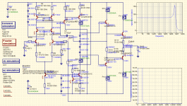
Unfortunately my software (ngspice) doesn't readily do Monte Carlo simulations. I tried varying the betas of various transistors and the offset changed the linearity remained good. At 1 kHz and +/-15 V supply, a +/-12 V sinusoidal output has -130 dB harmonic distortion below the fundamental.
The big flaw in the design is that the input offset is high, which I am not experienced enough to understand exactly why. I have included an offset control and output bias current control. But I don't expect it will be useful for DC amplification, probably a chopper amplifier needs to be used for that.
I would like to have high voltage op-amp so that it could be a component of a power amplifier or a piezo driver or something like that. Having output bias current control means that the output can either be low voltage and high current or high voltage and low current depending on requirements. I have a project
GitHub - profdc9/PowerAmpAudio: Power Amplifier based on Michael Chua's C300 amplifier
I based this opamp on, and I thought it might make a good building block as well as an example to study.
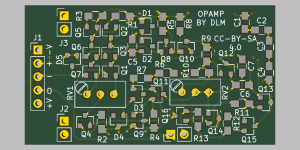
So I laid out a board for it that JLCPCB can populate using their process pretty cheaply, and the board is only 47 by 26 mm. Most of the wiring is on one side of the board with the other side being VCC and VEE. I hope this small size and short connections keeps parasitics low. There is a 47 pF Miller capacitor that may need to be increased if my layout is not good enough.
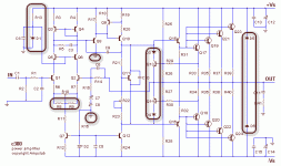
So the next time I put in an order I will probably have this made and try it out. Check out the schematic and picture of the PCB.
Thanks for your feedback (haha) and let me know any comments.
The big flaw in the design is that the input offset is high, which I am not experienced enough to understand exactly why. I have included an offset control and output bias current control. But I don't expect it will be useful for DC amplification, probably a chopper amplifier needs to be used for that.
I would like to have high voltage op-amp so that it could be a component of a power amplifier or a piezo driver or something like that. Having output bias current control means that the output can either be low voltage and high current or high voltage and low current depending on requirements. I have a project
GitHub - profdc9/PowerAmpAudio: Power Amplifier based on Michael Chua's C300 amplifier
I based this opamp on, and I thought it might make a good building block as well as an example to study.
So I laid out a board for it that JLCPCB can populate using their process pretty cheaply, and the board is only 47 by 26 mm. Most of the wiring is on one side of the board with the other side being VCC and VEE. I hope this small size and short connections keeps parasitics low. There is a 47 pF Miller capacitor that may need to be increased if my layout is not good enough.
So the next time I put in an order I will probably have this made and try it out. Check out the schematic and picture of the PCB.
Thanks for your feedback (haha) and let me know any comments.
Attachments
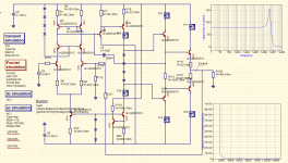
I would approach the whole circuit differently, but some things to consider....
It appears your bias current for the whole amplifier is set by resistors R6/7 (100k each) into D3/D4, so the amplifier bias will depend on the supply voltage from V+ to V-.
The earlier schematic had +/-100 volts supplies, but I would think the voltage of +/- 70V or less would be more inline with the BV limits of those transistors.
Q8 seems to be biased at a fairly low current level?
Putting a sink current on the diode string (D1/D2) biasing the Q3/Q6 would better define the cascode bias conditions. Look at your referenced circuit, below.
I do not understand the series connected capacitors C1/2/3/4, why not one capacitor?
One would prefer thermal coupling between Q12 & Q13/Q14/Q15/Q6. Also look at the your referenced circuit.
It might be good to look at all the collector currents and BJT Vce values again carefully. Calculate the Gm of each transistor, to see if it still makes sense to you.
Look at the circuit you referenced in the link from above & notice the red circled area below, which are different approaches from what you are doing.
Attachments
- Home
- Source & Line
- Analog Line Level
- a discrete LM833 ?