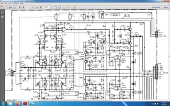
At least in simulation, the change in bias current in the stages when D3/D4 is +/-15 vs +/- 75 is very small, only 1.6 mA vs 1.7 mA, which does not seem to affect the distortion or gain.
Q8 is a common collector and the 10k resistor is there just to keep the transistor biased on. Most of the actual current is being drawn from the base of Q10.
One of the problems with making an op-amp vs a power amplifier is that I have no ground to use as a reference, only the supply rails. So R6/R7 must be tied to the top rails. Since I have access to only 0805 for this, I use two resistors R6/R7 to get a 1/4 watt power rating so that at full supply voltage the resistors are each dissipating 56 mW. Similarly, since I have access to 50 V capacitors, I need to use four of them to get a 200 V rating for the supply.
The resistors R12/R13 are intended to prevent thermal runaway. I can not find a good resource on how to calculate these, but I guessed that an approximate answer would be about 1/gm (26 mV/1 mA) approximately is 22 ohms. Cordell has a model for the transistors I am using and when I change the output transistors to be hotter (like 80C from 20C), the quiescent current does not change much with 22 ohm emitter resistors, whereas it does when the resistors are not present. The resistors are still small enough so that the output swing can drive headphones if needed if the supply is +/-15 V.
I have checked the currents in the transistors and they are about 1.5 mA quiescent except for the output stage which can be tuned to be larger if the voltage of the supply is lower.
I would approach the whole circuit differently, but some things to consider....
It appears your bias current for the whole amplifier is set by resistors R6/7 (100k each) into D3/D4, so the amplifier bias will depend on the supply voltage from V+ to V-.
The earlier schematic had +/-100 volts supplies, but I would think the voltage of +/- 70V or less would be more inline with the BV limits of those transistors.
Q8 seems to be biased at a fairly low current level?
Putting a sink current on the diode string (D1/D2) biasing the Q3/Q6 would better define the cascode bias conditions. Look at your referenced circuit, below.
I do not understand the series connected capacitors C1/2/3/4, why not one capacitor?
One would prefer thermal coupling between Q12 & Q13/Q14/Q15/Q6. Also look at the your referenced circuit.
It might be good to look at all the collector currents and BJT Vce values again carefully. Calculate the Gm of each transistor, to see if it still makes sense to you.
Look at the circuit you referenced in the link from above & notice the red circled area below, which are different approaches from what you are doing.
My 2 cents, going by the PDF schematic:
2N5551 is a relatively high voltage, but only medium beta part. Good for a cascode, NOT good for an input transistor. As hot as you're running the thing (why anyway?), that'll give you a crapton of input bias current and associated current noise. (I would start out with a tail current around 1 mA, so 500 µA a pop.) Probably why you had offset issues earlier, presumably your impedances were not matched.
With just a 1k pot, offset adjustment is likely to be very touchy. Current degeneration seems rather heavy anyway, so I'd consider 220 or 330 ohm emitter resistors in addition, and maybe a 2k or even 5k pot.
I don't like cascode bias too much. Vce for the input transistors is Vcc-5*Vpn, or not a great deal less than Vcc. I would rather have the bias diodes placed between cascode transistor bases and input transistor emitter midpoint, with a bias resistor to Vcc added to supply them. This would give you a bootstrapped cascode at a much lower input transistor Vce, so even a 2N5089 or one of its SMD versions could be used.
(Golden age Japanese transistor power amps tended to use cascoded JFET inputs with low-noise dual FETs, guess why.)
Current source diode string is floating in thin air.
In my experience simulating, buffered VAS setups have a habit of making the amplifier prone to common-mode distortion, so beware. A cascode may prove useful as well, but as always the more transistors you've got involved the harder it is to get things stable.
Consider higher-order compensation at least in a later iteration.
As mentioned, thermal coupling between input, current mirror, as well as all of bias spreader + output transistors is important.
5551/5401 are not likely to cut it as output transistors, I would suggest something beefier more in medium power terrain. MJE340/350, 2SD669/2SB649, BCX/BCP53/56, depending on what supplies you want. (Vceo rating should be >Vcc-Vee.)
Some consideration should be given to surrounding impedances in general. What do you expect in terms of source impedance? What makes sense in terms of loads and feeback network impedance? Design is always difficult if you don't have a target spec.
How does a bootstrapped cascode work? I thought that the whole idea of it was that the emitter of the common-base transistor held the collector of the common-emitter transistor at a constant voltage. Do you place a zener diode between one of the emitters at the bases of the cascode transistors? Maybe I should get rid of the cascode, as it doesn't seem to increase the open-loop gain much or the input impedance.
I was thinking I could put beefier transistors at the output of the amp if I needed to source more current, like embedding the amplifier into a feedback loop.
The reason I was running the input transistors with a lot of current is because the op amp was slew rate limited without it. With R2=330 ohm I can get 20 V/us, but only about 10 V/us with R2=680 ohm. Maybe this introduces too much noise? Is there any way to try to get the 2N5551 inputs to be quieter?
@profdc9
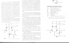
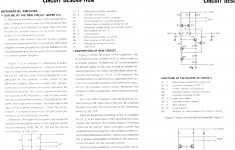
you get all the explanations and even a much more advanced version of biasing a bootstraped cascoded circuit in kenwood l-a1 service manuals.
KENWOOD L-A1 SM Service Manual download, schematics, eeprom, repair info for electronics experts
you get all the explanations and even a much more advanced version of biasing a bootstraped cascoded circuit in kenwood l-a1 service manuals.
KENWOOD L-A1 SM Service Manual download, schematics, eeprom, repair info for electronics experts
Attachments
Just another 2 cents .. (.. also from the PDF schematic)
I think the slew rate is being limited by a combination of two or three factors:
- the sinking CCS sets the VAS current at ~880uA -- too low
- the ratio of R5 to R8, 10k to 22r (455:1) is too high; it's discarding the current gain of the input stage and expecting too much of Q8; remember, Q3 and Q6 provide no current gain
- since Q8's Base is supplied by an extremely high impedance, C7 at 47pF is probably too big
Cheers
Slew rate should be affected pretty much only by two things, tail current and compensation capacitor C7. If an increase is desired, potential options would be either going JFET input (so tail current can be increased) or using 2nd-order compensation.
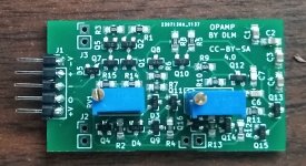
An update on the op-amp project.
I got around to testing the design and it seems to work both in the noninverting unity gain configuration and the noninverting gain of 11 configuration. I have tested it up to +/-30 V rail supply (which is high as my bench supply goes).
It is designed so that you can stack two of them and have the resulting stack fit in a DIP-8 socket with a two op-amp pinout.
The next version will have the ability to put a pair of medium power transistors on the PCB so that it can directly drive a pair of headphones or a power stage. of a power amplifier. The idea is to have the amplifier consist of this PCB, and driver transistors (like MJE15032/33) and power transistors (3281/1302) on a heatsink with a feedback network.
Attachments
- Home
- Source & Line
- Analog Line Level
- a discrete LM833 ?