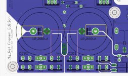
Im designing a crc psu for my gainclone and debating on whether to use a solid ground plane or a slitted one such as seen on myref fremen edition. On that board its clearly seen that the plane is slitted to where the return currents are forced to go between the negative pin of each smoothing cap.
Whats more curious to me tho is how the plane is then split all the way to the rectifiers. The myref im talking about is a double rectifiers design and thru that slit the + and - ends of the rectifiers that form the ground are seperated and only joined inbetween the smoothing cap.
I guess what im looking at is sort of a star ground arrangement? Id like to know what the merit would be for that vs the plain solid ground pour.
Just to be sure... are you referring to the slots in yellow, the ones in pink or both?

Attachments
Last edited:
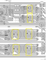
I didn't have any experience in PCB design when I've designed the FE's one so I've read everything I've found, seen dozens of service manuals and found that often japanese brands like Denon and Yamaha, sometimes also Sony and Marantz used those slits in ground pours, ground planes or even on thick traces, some examples:
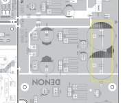
Denon DVD-5910

Sony SCD-XB940

Here on lower right interesting the slits between the capacitors ground terminals and the separation on ground lines.
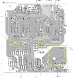
Sony SCD-XA5400ES

No planes or pours, a classic star ground and, yet, traces have slits around capacitors' pins...why?
Yamaha CD-S2000

Pioneer VSX1014

No ground planes, a normal star ground and yet on the ground pour between capacitors' pins they felt a slit was needed...why?
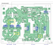
Marantz SR-5500

Again, no ground planes, a normal star ground and yet on the ground pour between capacitors' pins they felt a slit was needed...why?
And, also why the slits on the left (in yellow) and other traces without (in cyan)...
Some manufacturers do not use those slits at all, some others sometimes yes and other times not...
Nevertheless it made sense to me (I've seen it as way to make the capacitors more effective) and so I've did the same.
Maybe someone with more experience, like Marce, maybe, could shed some light on it.
Denon DVD-5910
Sony SCD-XB940
Here on lower right interesting the slits between the capacitors ground terminals and the separation on ground lines.
Sony SCD-XA5400ES
No planes or pours, a classic star ground and, yet, traces have slits around capacitors' pins...why?
Yamaha CD-S2000
Pioneer VSX1014
No ground planes, a normal star ground and yet on the ground pour between capacitors' pins they felt a slit was needed...why?
Marantz SR-5500
Again, no ground planes, a normal star ground and yet on the ground pour between capacitors' pins they felt a slit was needed...why?
And, also why the slits on the left (in yellow) and other traces without (in cyan)...
Some manufacturers do not use those slits at all, some others sometimes yes and other times not...
Nevertheless it made sense to me (I've seen it as way to make the capacitors more effective) and so I've did the same.
Maybe someone with more experience, like Marce, maybe, could shed some light on it.
Attachments

Yes, it is but notice that no 'dangerous' slots are made (AKA no traces cross those ground plane partitions)Im designing a crc psu for my gainclone and debating on whether to use a solid ground plane or a slitted one such as seen on myref fremen edition. On that board its clearly seen that the plane is slitted to where the return currents are forced to go between the negative pin of each smoothing cap.
Somewhat, yes, through ground planes partitioning a sort of star ground is formed.Whats more curious to me tho is how the plane is then split all the way to the rectifiers. The myref im talking about is a double rectifiers design and thru that slit the + and - ends of the rectifiers that form the ground are seperated and only joined inbetween the smoothing cap.
I guess what im looking at is sort of a star ground arrangement? Id like to know what the merit would be for that vs the plain solid ground pour.
Attachments
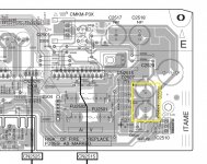
Hi Dairo. Mostly the pink. What im rlly curious about is why you split the rectifier returns
It's probably not necessary, currents would anyway follow the least impedance path but at the time it made sense to me.
Would I do it again? Maybe not but I don't see either a reason to modify it. 😉
Thats very interesting and im sure with a gokd reason to do so at the time. Ive only seen it done like that in a walt jung regulator drawing that was also from 70/80s. There he split the return rail all the way to the rectifier only joining them at the output cap into a very obvious star arrangement.
Still cant decide what would be the better choice cuz there seem to be no info on how the trace should be for double rectifier...
Still cant decide what would be the better choice cuz there seem to be no info on how the trace should be for double rectifier...
Im guessing the slit + no slit mixture for the marantz was done to keep the trace impedance equal at least right at the cap pin where it might matter the most? Because otherwise the traces for those 2 caps r very different width
Try to get 60uM boards at JLC instead of 30uM boards. This minimizes Resistances.
A gainclone will have good PSSR considering its a Chipamp, no need to get fancy.
A gainclone will have good PSSR considering its a Chipamp, no need to get fancy.
If you want to do it similar to mine do it without problems, no secrets, no rocket science, it simply works and measure well too... 😉Still cant decide what would be the better choice cuz there seem to be no info on how the trace should be for double rectifier...
I don't think so... you would want equal impedance in a balanced pair (like I did for the V+ and V- traces that goes parallel on ground plane with equal width) but for the return path what you want is the lowest possible impedance so very wide traces or better copper pours and even better a ground plane, in this last case some more care is neeeded.Im guessing the slit + no slit mixture for the marantz was done to keep the trace impedance equal at least right at the cap pin where it might matter the most? Because otherwise the traces for those 2 caps r very different width
And thick copper also helps lowering impedance as v4lve lover already noted.
I'm not sure that throwing a big fat ground plane for the ground return is the best approach (and that's why the slits are used), but one is free to do whatever he wants.
A solid copper plane is lower impedance than a slotted copper plane.
I tend to use a mix of copper pours and star ground system.
If there are no high current paths I just use a full pcb copper pour on each layer.
I tend to use a mix of copper pours and star ground system.
If there are no high current paths I just use a full pcb copper pour on each layer.
"If there are no high current paths I just use a full pcb copper pour on each layer. "
Well, I'm wondering what currents flow through the PSU - high or low 🙂🙂🙂
Well, I'm wondering what currents flow through the PSU - high or low 🙂🙂🙂
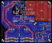
Another interesting approach is Olegsh one:
Thanks, Dario.
thats the other one i had in mind. I believe certain high end designs use that. theres basically no wasted copper with that arrangement
I'm not sure that throwing a big fat ground plane for the ground return is the best approach (and that's why the slits are used), but one is free to do whatever he wants.
Actually this is the best way of doing it. The rationale here is that the impedance of the ground plane is much lower compared to a significantly smaller ground trace thus the error potential generated by the ground return currents is significantly minimized by a large ground plane. On top of that the inductive component of the impedance of a power trace over the ground plane is lower too which further improves the situation by minimizing not only the error potential but also the radiated noise. Next, if wide power traces on top of a ground plane are used one gets the lowest impedance in the power path possible. Now, one has a choice to contain the high current bursts charging the filter capacitors by placing a high impedance in a desired location: well known CR(L)C arrangement. Exactly this is done in my PCB design in post #13. Thus, the ground potential becomes more and more stable as you go from left to right of the PCB: from the AC input to the clean DC output.
Now, if the space is tight, so the distance from the "dirty" ground to the "clean" ground is short, one can introduce extra impedance in the ground return path preventing high current capacitance charging bursts from entering the "clean" ground area. This is where the slits in the ground plane can be used. In Dario's My_Ref Fremen Edition PCB design all the charging pulses from the rectifiers to the big filter capacitors are contained in a small area between these capacitors and the rectifiers thus minimizing the radiated noise and the error potential where the output ground and feedback ground reference are taken.
Regards,
Oleg
- Home
- Amplifiers
- Power Supplies
- Slitted ground plane?