Oleg, can you tell me to which point are attached the ground pin of the regulator (actually where the internal reference voltage is connected to ground) and the same - for the resistor from NF voltage divider?
Regards
Alex
Regards
Alex
The ground pin of the reg is connected to its thermal pad (look at the upper right pin of both ICs) and the ground leg of the feedback voltage divider (left edge of R1 and R2) is right next to the IC package.
Regards,
Oleg
Regards,
Oleg
Yes, I can see this 🙂. My question is: referring to your electric schematic, to which point of it these pins are attached?
I don't understand the question. On the schematic diagram all ground pins connect to the GND symbol 🙂
Yellow rectangles show good low-noise PCB design examples.Again, no ground planes, a normal star ground and yet on the ground pour between capacitors' pins they felt a slit was needed...why?
And, also why the slits on the left (in yellow) and other traces without (in cyan)...
🙂 So, according to you, since the GND is on the whole bottom layer's ground plane, there's no difference where the internal REF and the feedback's resistor will be attached.
However, this is not the optimal approach according to the PSRR and noise performance. These two nodes must be attached to an unequivocal and steady point of the ground.
You stated that the currents will follow the least inductance path but I'm afraid it's not always the case. In the past I also thought this is the right approach and just placing a big ground plane for the ground return will do the job until the reality punch me in the nose (badly 🙂).
I designed a PCB for one of my headphone amplifiers and the idea was to have output stage biased at 200mA constant current (deep in the class-A region).
I threw a big fat ground plane on the bottom side and was glad with my routing. In the process of setting the amp, it turned out that when the overall currents drawn by both channels goes above certain threshold, an audible hum appeared on the headphones and on the spectrum analyser.
When the currents were lowered below the threshold, the hum was almost not audible, but still visible on the spectrum analyser (although with not so high levels of harmonics).
Then I went to a friend for auditioning and (possible) advices.
I explained the problem and after a short wondering about wires, the pot etc., he detached the board from the fixing spacers, turned it upside down and when he saw the ground plane on the bottom, he whispered "Oh, man, it's totally wrong!". Then he asked me if I'm going to sacrifice the board in order to understand how the things must be done. I didn't mind, the took out his Dremel and after 15 min. of noisy scratching on the PCB and soldering a new wires between different points, he returned the board to me, I set it back, turned the power on and... yes, the amp was dead silent.
I was so ashamed that the only thing I did was to shook his hand.
It was an important lesson for me (and an expensive one - the boards are big enough and for 5 pcs. I paid around $60-70).
I'm attaching here the pictures of a brand new board with a shiny big fat ground plane for the ground return and the "reworked" one.
Anyone can make his own conclusions.
Attachments


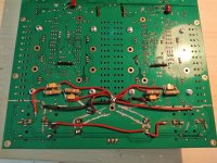
Am I missing something? Or maybe you are missing something? 😕Yellow rectangles show good low-noise PCB design examples.
I use those same slits in my design, and I was illustrating to the opener that those were used in several hifi products.
What I don't know is the inner working of those slits, it seems that you know it, can you shed some light on them, on how and why they work?
Thanks in advance 🙂
arpagon, I hope you understand that your PCB is not a generic example and thus you can't generalize your single PCB design experience on any other PCB design. Using the ground plane also needs care. For example if power return path overlaps with the signal return path for an extended length on the PCB an increased hum is not a surprise. Simply using the ground plane and paying no attention to power and signal routing is not going to work well. One should carefully consider a number of factors even if using the ground plane. Often one uses two separate ground pours, one for the sensitive signal area and another for the high power area and connects them in a single carefully chosen point. So there is more to it than just flooding the bottom of the PCB with a ground plane.
Last edited:
Oleg, call me Alex (or Aleksandar), please. Of course I'm not claiming that my board is the ultimate and the only possible design, I just want to stress that when you design a linear PSU, the abovementioned nodes (ground connections of the Vref and the NFB divider) MUST BE connected to a well-known steady point from the ground return path, not "in the middle of nowhere" where is the case with the simple ground plane. The ground plane can be more or less acceptable when the currents are low but once the currents go high, the problems with the ground plane appear.
Choosing the right point for the star center ground is also a bit of magic 🙂, but in a case of bi-polar PSU I suggest an artificial point as closer as possible to the output terminal's GND pin.
For uni-polar PSU this center must be attached to the ground leg of particular filtering capacitor, can you guess which one is the right choice - the input capacitor after the bridge rectifier or the one on the output?
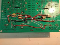
Current has to have its way only through a capacitor pin, but not far from pin. We can't put cap pins everywhere we need, but we may move PCB wires so they led current through a cap pin.What I don't know is the inner working of those slits, it seems that you know it, can you shed some light on them, on how and why they work?
Last edited:
Its all electrickery.
The main object with star ground and copper pours is to screen and keep high/medium power return paths away from small signal paths.
The high power stuff modulates the ground and if not laid out right the small signal ground too.
One of my early designs was a USB mixer.
Naively I just threw down the pcb in what ever way the tracks appeared.
When it came back the thing had 1VRMS on output with input shorted !
When I drew out what I had the power supply mixed in with small signal ground.
The charging impulses into smoothing caps was modulating the small signal ground and injecting hum which was amplified.
So I re-laid out pcb with power supply separate on the pcb and it worked a treat.
Last edited:
Thanks for the answer 🙂Current has to have its way only through a capacitor pin, but not far from pin. We can't put cap pins everywhere we need, but we may move PCB wires so they led current through a cap pin.
So I was not far:
Nevertheless it made sense to me (I've seen it as way to make the capacitors more effective) and so I've did the same.
Still no word on whether split plane for voltage return positive and voltage return negetive is better or not.
My hunch is that because the positive and neg supply rail modulate the current ever so differently, if their grounds r shared their modulation will fight eachother and affect their output whereas when split til the rectifier return the modulation will be contained and the overall ground quieter, tho with higher impedance.
My hunch is that because the positive and neg supply rail modulate the current ever so differently, if their grounds r shared their modulation will fight eachother and affect their output whereas when split til the rectifier return the modulation will be contained and the overall ground quieter, tho with higher impedance.
Last edited by a moderator:
Dario please have a look at AMP???? Amp Repair Studio. Its evident from photo documents that even the japanese high end gears all used the same slit and split tracing as you showed earlier here. Sansui au-11 for example splits the ground plane all the way down to the rectifiers. I dont believe these japanese designers of the yesteryear were novices. Quite the contrary infact, and as we've been reinventing the wheel we probably chose to forget some of the details that mattered to these people.
- Home
- Amplifiers
- Power Supplies
- Slitted ground plane?