So I'm trying to use a simple current mirror to provide a voltage-independent 5mA minimum load and, like, well, I can't get it to work - I've spent more time on this than I'm willing to admit so if someone could lend a hand that'd be great.
Basically, I've got a 15V rail and a variable voltage (~0V to ~25V) rail that I want to sink 5mA from. I've tried with NPN BJTs (2N3904) and NMOS FETs (2N7000), all with the same result - everything is all good on "input" side, but the current just rises on the mirroring side, going up to 200mA in a couple seconds with the BJTs and much slower with the FETs.
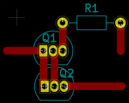
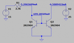
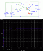
Attached are schematic and a quick sketch of how I've wired them up.
What am I missing?
Basically, I've got a 15V rail and a variable voltage (~0V to ~25V) rail that I want to sink 5mA from. I've tried with NPN BJTs (2N3904) and NMOS FETs (2N7000), all with the same result - everything is all good on "input" side, but the current just rises on the mirroring side, going up to 200mA in a couple seconds with the BJTs and much slower with the FETs.
Attached are schematic and a quick sketch of how I've wired them up.
What am I missing?
Attachments
Last edited by a moderator:
Thats a very wide voltage compliance range required of Q2. Can be mitigated with the addition of identical emitter resistors to each to improve the output impedance.
Alternatively, use the 3 transistor Wilson current mirror.
Alternatively, use the 3 transistor Wilson current mirror.
In real life or in the sim?
My simulation works "right". I do not have any little BJTs handy for proof.
Are you sure of your device pin-outs?
In real life. My sim "works" too - I attached it. I'm sure to the best of my ability which is why I posted the layout, but I did try it with like 15 different BJTs soldered in 2 different circuits, and on 2 different breadboards, with 2 different multimeters, etc etc.
Last edited by a moderator:
Think your power dissipation in the output transistor is high at 3.6 watts. Seems like thermal run away in that device.
Think your power dissipation in the output transistor is high at 3.6 watts. Seems like thermal run away in that device.
How are you getting 3.6watts with 6mA of current?
Oops sorry,200 ma was your final current. 6 ma would give .1 watts, still may be a bit high without emitter resistors .
BITs are notoriously thermally unstable with a fixed base voltage bias which is essentially what the input transistor is generating. MOS quite a bit better as you have observed.
In simulation where the same model is used and integrated circuits where the substrate is evenly doted, one can assume identical characteristics from individual components. With same type components from one batch, one must degrade the ideal performance by adding resistors to the emitter. A 10:1 ratio compared with the medium internal re will suffice in most cases.What am I missing?
re ~ 25mV/Ie, so Re ~ 250mV/Ie (or 250mV/Ic).
Are you attributing this behavior to manufacturing imperfections?In simulation where the same model is used and integrated circuits where the substrate is evenly doted, one can assume identical characteristics from individual components.
You've got me a bit confused here, can you clarify perhaps with an example? Thanks.A 10:1 ratio compared with the medium internal re will suffice in most cases. re ~ 25mV/Ie, so Re ~ 250mV/Ie (or 250mV/Ic).
I couldn't agree more. My background is largely with ICs. Even then you have to be careful with the assumption that components are identical. Spice will assume this unless you force it otherwise. Modeling thermal effects requires even more manipulation. And then you need to know when it needs to be applied.
Emitter degeneration is almost magic when applied for the right reasons. I like your rule of thumb, but it is not always optimum. Still when used will usually prevent one from having a problem like this.
Always keep in mind that Vbe is reduced with temperature, and Beta gets larger. This leads to thermal run away without some mechanism to prevent it.
Your input transistor is dissipating about 2.5 mW. (0.6*.005). Your output transistor is dissipating about 90 mW. (18*.005). As such, they will no longer behave identically unless their temperature at the die level can be forced to be equal. Generally, this can only be accomplished if they exist monolithically.
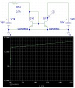
OK with some more testing the thermals do seem to be issue - it doesn't seem to happen with V2 at 1V. At 25V the dissipation on Q2 would be ~125mW so some kind of different solution is needed.
Contrary to my earlier post, the Wilson doesn't work "perfectly" either - 5mA is maintained through Q2 only down to 0.8V, which isn't low enough. Interestingly LTSpice doesn't reflect this in a Wilson-only sim, but when I sim a greater circuit with the Wilson minimum load integrated (attached), it breaks below 5mA at ~0.8V (R6 at ~300ohms) same as the real live circuit.
To not go off topic, I'll probably make a separate post about minimum loads in Testing & Equipment.
Attachments
Last edited by a moderator:
Without digging into your application for the current source, both Wilson and the use of degeneration will reduce headroom with respect to the negative rail. With 250 mV of degeneration and transistor Vce sat of .15 volts, the output will be reasonably close to desired to within .4 volts of the negative rail.
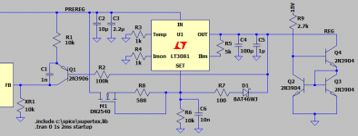
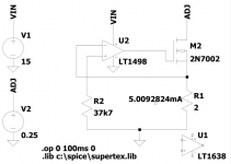
In context of a power supply, you can "afford" more than a 2-Q current source. Put any dang opamp in the loop and it gets better.
The "10mV battery" is obviously a divider, adjustable for opamp offset error. V22 is any supply to keep the opamp alive, maybe somewhat stable.
This run also sweeps Temperature 0 25 125 deg C. I was puzzled that there is a variation, but then realized we are controlling Ie when we want constant Ic. The difference is hFE and Ib. The difference is small and there are billions of trivial complications to avoid this error. Today a MOSFET makes sense. (My antique sim lacks small MOSFETs.)
Attachments
Nothing is obvious to me...not sure if I wired it right but seems to work very well though, 25mV to 25V only the Opamp seems thermally affected at 30mW. LT1498 is a "bit" overkill, I think, just what I have on hand that's in the sim.The "10mV battery" is obviously a divider, adjustable for opamp offset error.
I'll try it out tomorrow, thanks.
(screenshot says 250mV oops but it's the same at 25mV)
Attachments
Last edited by a moderator:
In general: Y/Yo=(e)exp(X/Xo){Xo=kT/q}You've got me a bit confused here, can you clarify perhaps with an example? Thanks.
Specific: kT/q = 25mV at room temperature. (Yes depends on more, but ROT.)
- Home
- General Interest
- Everything Else
- Problems with simple current mirror