Fine but what are your arguments?
My arguments for simple 2-stage follower (emitter follower+source follower) are:
1. Absence of local feedback that must be switched on/off twice every period in AB-class operation.
2. Easy to thermostabilize driver stage.
3. Only current gain, so no interaction with load impedance up to some MHz.
4. Intrinsic low output impedance and well-balanced shoulders allow to easily hold output zero.
5. Comparatively high input impedance and very low input capacitance (in case of ksc3503/ksa1381) allows to pick huge and wide gain from VAS output.
6. Comparatively high widebandness even at low driver idle current, 10 mA are fast enough for any audio application.
7. Mostly immune to rail variation under heavy load.
8. Both flanges at same output voltage, allow huge copper heat spreader.
An emitter follower is a buffer where the negative feedback and the output are the same pin, ie the emitter/source. But the transistor current does react to the load back-emf and impedance. The load impedance is reflected in the input impedance for BJTs, not so much for FETs.
A big advantage of an EF is that the output impedance is very low and very wideband, stable under no load, vs a CFP which will oscillate without proper compensation, usually a Zobel network.
But there is also the fact that it is easy and effective to cross-couple an EF, which prevents shoot-through currents when driven at high frequencies. This has been the root cause of many amplifier failures in the past. A CFP topology has only passive resistors to pull the outputs off, which is slow and leaves one side still conducting heavily as the other is turned on. This is particularly a problem coming out of clipping and ironically can be avoided by amps that have a poor output saturation voltage, ie if the outputs can not be driven into saturation.
ok, a quick update, the first cct buffer driver worked ok.
the second cct complimentary pair seems to have a stability issue, a 0.4vpp square has around 50mVpp of noise on the flats and without a zobel breaks into full osc.
i varied the base R's and R16/24 but with the same results.
the second cct complimentary pair seems to have a stability issue, a 0.4vpp square has around 50mVpp of noise on the flats and without a zobel breaks into full osc.
i varied the base R's and R16/24 but with the same results.
You should go for a nice sounding three stage topology without any voltage followers. Reverse the device polarities.
The VAS buffer is an English gimmick that lacks foundation.
The VAS buffer is an English gimmick that lacks foundation.
Hitachi created a lat fet datasheet circuit that just used a double LTP to drive the output lat fets. Maplin used it for about 10 years on various models of their lat fet power amplifier.

Why not ? Maplin sold many hundreds.That`s a very different approach. I don`t recommend it.
ok, a quick update, the first cct buffer driver worked ok.
Have no worries, this is a well-known, reliable and deeply investigated approach.
the second cct complimentary pair seems to have a stability issue, a 0.4vpp square has around 50mVpp of noise on the flats and without a zobel breaks into full osc.
i varied the base R's and R16/24 but with the same results.
A common source OPS are discussed wildly around the web. There are no critical benefits in terms of heat dissipation, but very much problems in terms of understanding how it works and how to work with it. Let me point your eyes.
1. Huge output resistance of drains in a common source output config straightly demands huge feedback loop depth to minimize output resistance of the whole amp to allow it to interact with load.
2. Gates must be driven relative from hugely variable power rails because voltage regulation of such a rails is again a not less comprehensive amp with same current rating.
3. Just compare input capacitance seen from driver stage. Follower (common drain) N+P has a typical capacitance of ~150 pf for one pair and easily drives by small and fast 3503/1381, while common source demands for driving relatively huge Ciss at ~500/700 pf each device.
4. The main concept of the amps demands as much feedback depth as you can cope. This asks for a high-impedance low-capacitance point somewhere in the amp. With a shown in post #2 2-stage follower you can obtain such a point with easy and with a good resistance and capacitance ratings. Common source will anyway have much lower input impedance and demands for additional stage for VAS load decoupling.
5. Just draw and compare wingspreads for such a stages being driven from a high-impedance source (like VAS output, some ~100-300 kOhms). The point of interest - is a closing shoulder in AB-class operation. In a compound pair output device used with a gain and amplifies driver stage, but closing output device asks for driver stage to interact with load for a short time. This hugely drops input resistance of such a stage, which in case, asks for a some kind of follower to interact with a VAS output and, of course, huge bandwindness to correct this very fast transients.
6. Common source OPS have intrinsic 2-stage feedback turned on and off at each shoulder. This provide you with a need to understand bandwindness of such an errors and take precautions to keep feedback loop from saturation.
So, reread post #21, use follower and have no doubt.
All this is vague nonsense, as I see it.
Very comprehensive and valueable input!
But will we see any adequate arguments from your point of view?
Just a parenthetical -- when Troy Huebner wrote the application note for Nat Semi (subsumed into TI) he demonstrated that the gate stoppers in the lateral mosfets can be adjusted to optimize THD%.
What conclusion did he draw?
See Texas Instruments Application Note 1645, page 14 == slightly overdrive the amplifier with a square wave and adjust Rg on the output MOSFETS until the slope of the input and output are parallel.
Thank you. That`s a rough general formula, the charge distribution over frequency not being taken into account. We are left with the possibility to intuitively determining the gate and source resistor values.
The insulated gate interface presents a light load enough to be driven by a common emitter amplifier, but is a source of considerable distortion. A high input impedance does not give low distortion, as widely believed. The instability mainly stems from the combination of short channel length, heavily doped source region and high operational speed. The gate resistor, just like the source resistor, reduces charge velocity, but in different frequency bands, the one does not "eliminate" the need for the other.
The insulated gate interface presents a light load enough to be driven by a common emitter amplifier, but is a source of considerable distortion. A high input impedance does not give low distortion, as widely believed. The instability mainly stems from the combination of short channel length, heavily doped source region and high operational speed. The gate resistor, just like the source resistor, reduces charge velocity, but in different frequency bands, the one does not "eliminate" the need for the other.
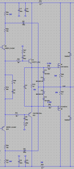
PP VAS
A version of this circuit comes in the LTSPICE
C:\Program Files\LTC\LTspiceXVII\examples\Educational\100W.asc . I like this circuit but it has two issues that are ~easily fixed.
1. The VAS current is dependent on the LTP current, which in the circuit you show is supply voltage dependent. The LTC circuit partly fixes that with a current source on the (1st) LTP but I prefer to limit the current in the VAS LTP as well by replacing R4,R5 with two transistors and emitter resistors, bases fed by R10, so that the VAS LTP total current is always ~R10/0.7V.
2. The VAS clipping/saturation voltage is a volt or two more than it needs to be and that adds to the "on" gate voltage of the fets so that the output saturation is about 6 Volts from the rail, too much. The solutions to this are variation of partial boost-strap arrangements and NOT running the VAS current through the fet bias circuit. ie using a separate current for that bias. You can drive the middle of the FET bias from the VAS, or drive one side of the fet bias and partial boot-strap that side of the VAS, or you can run the VAS from boosted supply rails. The fet bias current can be very small because the DC input to the FETs is ~zero and the AC coupling between the VAS and fets is a partial boot-strap.
Hitachi created a lat fet datasheet circuit that just used a double LTP to drive the output lat fets. Maplin used it for about 10 years on various models of their lat fet power amplifier.
A version of this circuit comes in the LTSPICE
C:\Program Files\LTC\LTspiceXVII\examples\Educational\100W.asc . I like this circuit but it has two issues that are ~easily fixed.
1. The VAS current is dependent on the LTP current, which in the circuit you show is supply voltage dependent. The LTC circuit partly fixes that with a current source on the (1st) LTP but I prefer to limit the current in the VAS LTP as well by replacing R4,R5 with two transistors and emitter resistors, bases fed by R10, so that the VAS LTP total current is always ~R10/0.7V.
2. The VAS clipping/saturation voltage is a volt or two more than it needs to be and that adds to the "on" gate voltage of the fets so that the output saturation is about 6 Volts from the rail, too much. The solutions to this are variation of partial boost-strap arrangements and NOT running the VAS current through the fet bias circuit. ie using a separate current for that bias. You can drive the middle of the FET bias from the VAS, or drive one side of the fet bias and partial boot-strap that side of the VAS, or you can run the VAS from boosted supply rails. The fet bias current can be very small because the DC input to the FETs is ~zero and the AC coupling between the VAS and fets is a partial boot-strap.
Last edited:
Hitachi created a lat fet datasheet circuit that just used a double LTP to drive the output lat fets.
The main disadvantage of this scheme goes from a relatively low lateral FETs transconductance. So for a case of a relatively hard 4 Ohm load VAS will be already saturated while OPS can't reach even -10 from rail voltage. This will result in an excessive heating of a subtle LatFETs working to a reactive load at excessive supply voltage.
The better way is to use higher rails or use bootstrapped VAS.
Also this scheme lacks in picking all available gain in such a 2-stage core.
First stage must be loaded to a current mirror, then gain must be raised by a follower before second LTP, of course, that ugly 27 pFs must be omitted and, again of course, VAS output must again be buffered with a follower/driver stage before LatFETs.
Doing this will provide you with additional at least 40 dB of feedback depth, lower distortion and more safe OPS operation.
- Home
- Amplifiers
- Solid State
- driving lateral mosfets