Hello all, I have a model Nineteen receiver that is doing excellent with the exception of one channel having offset that is all over the place. It fluctuates between -150mV and +150mV while the other channel is at 5-10mV. I removed all of the transistors from the board And measured them with a Peak Atlas DCA75 meter and they all measure okay, though they’re being measured a very low voltages. The electrolytics are new and the carbon comp resistors were replaced.
Could it be caused by something other than a transistor? A diode? A ceramic cap?
Anyways, here are the transistors on the board per manual.
34-1004
34-1005
34-1007
34-1014
MPSA56
Unfortunately Marantz part numbers make it hard to cross reference parts lol.
For the 34-1004 and 34-1005 Ive read the 2N5320 and 2N5322 would make good replacements. If that’s true, how about the MJE243 and MJE253? Specs would say they’d be equal or better.
For the 34-1007 Ive read the 2N3906BU is a good option and I have plenty of those.
For the 34-1014 Ive read the KSC945C is an option. I don’t have any of those, but have read in certain circuits the KSC1845 is good and in others the
Does anyone have a good suggestion for the MPSA56? I have a large number of transistors and hope I have something on hand.
I only really plan on replacing the transistors creating the issue. Are any of the transistors here supposed to be hFE matched? (Differential pair)
If anyone could point me in the right direction on where to start I’d be very grateful. If you’re ever in Oregon I’ll owe you a drink.
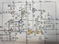
Here is a pic of the circuit and have colored the transistors
34-1004 Blue
34-1005 Green
34-1007 Red
34-1014 Orange
MPSA56 Purple
Thank you,
Dan
Could it be caused by something other than a transistor? A diode? A ceramic cap?
Anyways, here are the transistors on the board per manual.
34-1004
34-1005
34-1007
34-1014
MPSA56
Unfortunately Marantz part numbers make it hard to cross reference parts lol.
For the 34-1004 and 34-1005 Ive read the 2N5320 and 2N5322 would make good replacements. If that’s true, how about the MJE243 and MJE253? Specs would say they’d be equal or better.
For the 34-1007 Ive read the 2N3906BU is a good option and I have plenty of those.
For the 34-1014 Ive read the KSC945C is an option. I don’t have any of those, but have read in certain circuits the KSC1845 is good and in others the
Does anyone have a good suggestion for the MPSA56? I have a large number of transistors and hope I have something on hand.
I only really plan on replacing the transistors creating the issue. Are any of the transistors here supposed to be hFE matched? (Differential pair)
If anyone could point me in the right direction on where to start I’d be very grateful. If you’re ever in Oregon I’ll owe you a drink.
Here is a pic of the circuit and have colored the transistors
34-1004 Blue
34-1005 Green
34-1007 Red
34-1014 Orange
MPSA56 Purple
Thank you,
Dan
Attachments
The 500 piece minimum order for the 5320/5322 has got to hurt - yeah, I’d be looking at TO 126’s too.
KSA708 is an MPSA56-ish part. Careful with these, as there are both EBC and ECB basing options, depending on suffix. I’ve switched over to these, as ON has EOL’ed the A06/A56 in TO-92 (SMD versions still available), and all the 2nd sources want too much for them.
KSC945 is essentially a 2N3904 with ECB basing. But of course the more advanced types like the 1845 will *work*. I think the C945/A733 have been EOL’ed too.
Nothing suggests a bad transistor.It fluctuates between -150mV and +150mV while the other channel is at 5-10mV. I removed all of the transistors from the board And measured them with a Peak Atlas DCA75 meter and they all measure okay, though they’re being measured a very low voltages. The electrolytics are new and the carbon comp resistors were replaced.
Please do not replace parts at random.
It maybe some thingie in that board or not even that but in any case diodes and ceramic caps would not explain that either.Could it be caused by something other than a transistor? A diode? A ceramic cap?
You need to do some troubleshooting which implies knowing how the circuit works and what as_audio suggests may be way more possible.
A dirty scratchy worn adjustable resistor is a much more likely suspect.
Again: pulling parts at random , measuring them outside and trying to find the "bad" one by sheer chance (IF there is a bad one to begin with) is the worst way possible.
Statistically, rigged roulette or marked poker cards give you way better chances, go figure.
Instead of going after Transistors, check R1235 VR, R1221 VR R1226VR and as already as_audio have placed it, R1212
You need to check continuity for them as well as Contacts
Also check Temps on the HEATSINK of the Output..
You have a schematic, so measure voltage corresponding to what you can see in the schematic. Those should be very close what you read. also first is always first, Rail Voltages for feeding Voltage of the Amplifier..
And as you have another channel which is working correct you also can compare by checking each part and compare it to the other Channel..
Also last but not least, check soldering of the board for bad solder spots..
I'm sure you will find what's wrong.
Last edited:
Agree and add, this is one of the few cases where I recommend straight substitution with fresh parts.
Even if they "test good", variable resistors depend on a flimsy contact just touching a very thin carbon track under low pressure(contact elasticity), so dust/fluff/cigarette smoke can affect it, also contact atmospheric corrosion.
Justy be certain to set replacements to the same position and confirm with voltage checks.
Last edited:
Agree with both. No random or general parts exchange.
But your Marantz now already lost its collector value ?
Oscillation may be an issue - do you own a scope ?
But your Marantz now already lost its collector value ?
Oscillation may be an issue - do you own a scope ?
Have a look at R1212 and other variable resistors.
The 500 piece minimum order for the 5320/5322 has got to hurt - yeah, I’d be looking at TO 126’s too.
KSA708 is an MPSA56-ish part. Careful with these, as there are both EBC and ECB basing options, depending on suffix. I’ve switched over to these, as ON has EOL’ed the A06/A56 in TO-92 (SMD versions still available), and all the 2nd sources want too much for them.
KSC945 is essentially a 2N3904 with ECB basing. But of course the more advanced types like the 1845 will *work*. I think the C945/A733 have been EOL’ed too.
Nothing suggests a bad transistor.
Please do not replace parts at random.
It maybe some thingie in that board or not even that but in any case diodes and ceramic caps would not explain that either.
You need to do some troubleshooting which implies knowing how the circuit works and what as_audio suggests may be way more possible.
A dirty scratchy worn adjustable resistor is a much more likely suspect.
Again: pulling parts at random , measuring them outside and trying to find the "bad" one by sheer chance (IF there is a bad one to begin with) is the worst way possible.
Statistically, rigged roulette or marked poker cards give you way better chances, go figure.
Instead of going after Transistors, check R1235 VR, R1221 VR R1226VR and as already as_audio have placed it, R1212
You need to check continuity for them as well as Contacts
Also check Temps on the HEATSINK of the Output..
You have a schematic, so measure voltage corresponding to what you can see in the schematic. Those should be very close what you read. also first is always first, Rail Voltages for feeding Voltage of the Amplifier..
And as you have another channel which is working correct you also can compare by checking each part and compare it to the other Channel..
Also last but not least, check soldering of the board for bad solder spots..
I'm sure you will find what's wrong.
Agree and add, this is one of the few cases where I recommend straight substitution with fresh parts.
Even if they "test good", variable resistors depend on a flimsy contact just touching a very thin carbon track under low pressure(contact elasticity), so dust/fluff/cigarette smoke can affect it, also contact atmospheric corrosion.
Justy be certain to set replacements to the same position and confirm with voltage checks.
Agree with both. No random or general parts exchange.
But your Marantz now already lost its collector value ?
Oscillation may be an issue - do you own a scope ?
Thank you all for the suggestions, it saved me a good amount of time on swapping out transistors that were perfectly fine. I pulled R1212 along with others and sure enough there was an issue with R1212. It would not give me a stable resistance reading. I put in a new 25 turn Bourne and it revealed a new issue. I could not get offset below 100mV. Looking at the differential pair I found one of the transistors to be faulty. I put in a brand new matched pair of 2N3906BU, did the same to the other channel, and now have a very steady offset on both channels under 1mV.
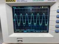
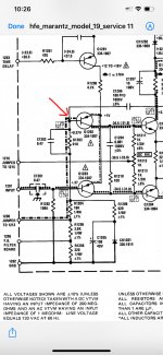
I’ve run into a new issue that was revealed. The bottom side of the waveform on channel B is severally distorted/clipped. I started by measuring the input of both channels and figured I’d work my way through the circuit. At the input of each channel the sine wave looks perfect.
I moved to the base of Q1203 on each channel and both channels look perfect. I then moved to the other transistor in the differential pair and measured at the base of Q1202. This is where I saw first evidence of the issue. The signal on channel B at the base of Q1202 is severally clipped on the bottom half while being perfect on channel A. I’m trying to figure out what is causing it. I don’t know exactly how the circuit works and where that signal is coming from exactly. It looks like the clean input on the driver board doesn’t feed Q1202?
On the schematic attached I marked in red where I am first seeing the distortion.
Dan
Attachments
In order to see what is going on :
Display one full cycle only (set osc. to 1100 Hz).
Show the output waveform in comparison.
This is sort of clipping. Check the voltage where it sets in.
Or is it independent of level ? Give us a hint about the levels.
Check dc voltages in comparison to the schematic.
Display one full cycle only (set osc. to 1100 Hz).
Show the output waveform in comparison.
This is sort of clipping. Check the voltage where it sets in.
Or is it independent of level ? Give us a hint about the levels.
Check dc voltages in comparison to the schematic.
Last edited:
The form of clipping indicates neg supply is limited somewhere.
Sorry current output stage is not shown in your schematic.
Did you change position of R1231 ?
Sorry current output stage is not shown in your schematic.
Did you change position of R1231 ?
Last edited:
In order to see what is going on :
Display one full cycle only (set osc. to 1100 Hz).
Show the output waveform in comparison.
This is sort of clipping. Check the voltage where it sets in.
Or is it independent of level ? Give us a hint about the levels.
Check dc voltages in comparison to the schematic.
Hopefully I’m doing what is asked of me, I set my oscillator to 1100 Hz and then adjusted the display of my scope to show one full waveform only. One pic of just when the clipping starts and one where it’s a little more severe.
The voltage where it sets in? Do you mean the output voltage? The clipping starts right at about 5 V output, into an 8 ohm load about 3.125 watts. Below that it is clean, hopefully that’s what you were asking. I checked voltages throughout the driver board. At the perimeter of the board schematic it shows voltages at
1203-Time delay, +26.5V (measured +26.9V)
1204- +28V (measured +28.2V)
1209- +36V (measured +37V)
1215- -36V (measured -37)
1207: + Base (measured +1.23V)
1208: - Base (measured -1.18V)
1210: + Emitter (measured +36.9V)
1214: - Emitter (measured -36.85V)
Anywhere else that you suggest I measure?
The form of clipping indicates neg supply is limited somewhere.
Sorry current output stage is not shown in your schematic.
Did you change position of R1231 ?
Excellent advice, negative supply issue. Unfortunately I cannot find a schematic of the entire thing, but I am attaching the schematic of the outputs. I did not touch R1231. I want to do as little as possible to this so that I don’t mess with the voltages too much as I don’t have a distortion analyzer. If I replaced the load line trimmers with new 25 turn ones I should be good as long as I set the value of the new one to be the same as the old correct? Is it possible that it could be a faulty trimmer causing this? Man, a Nineteen full of faulty trimmers lol.
Dan
Is the output distorted without a load connected? No load, no distortion, the problem should be in the output stage. The amplifier should be good up to and including the drivers.
Craig
Craig
Here is the output stage, drawn in a very unusual way.
Check all resistors first.
Seems the voltages are fine. I do not see your attachments.
I apologize, the attachment I meant to pass along was actually the output schematic that you posted. Don’t know how I forgot to link it. I will check the resistors.
Is the output distorted without a load connected? No load, no distortion, the problem should be in the output stage. The amplifier should be good up to and including the drivers.
Craig
Hi Craig. With no load it is still distorted, but the distortion starts a little earlier, at about 3.5V output. Once it sees an 8 ohm load it starts at 5V output.
Dan
I checked all of the resistors on the output board and the all measure good, I replaced a couple of them before as they were carbon comp.
Could it potentially be one of the large diodes mounted to the heatsink? Bias trimmer? Hmmm, I’ll keep at it.
Dan
Could it potentially be one of the large diodes mounted to the heatsink? Bias trimmer? Hmmm, I’ll keep at it.
Dan
Attachments
I’ve got it definitely pinned to the driver board. I desoldered all of the wires going to each driver board and swapped them, channel A going to B and channel B going to A. Prior to installing the boards I went through a flower all of the solder points just incase. Sure enough the clipping issue is now on channel A, so it swapped sides.
Not sure if anyone will find this info useful at all or if it’ll give any insight on what’s going on. After swapping the boards I powered it up on a dim bulb tester first just in case there were any shorts or anything. While on the DBT both channels made an equal 10V output and then both channels clipped the exact same. Once the receiver is directly on line voltage the good channel makes 57 watts (21.5V) output before any clipping and the bad still only makes it to 5V before the bottom of the wave form clips.
Dan
Check Q 1204, L 1203. You may also suspect an error in the "load line adjust"
circuitry which seems to be the current limiter, but you wrote that clipping
occurs without load also. Is Q 1207 conductive ? Check voltage on R 1221,
about 1.2 V.
circuitry which seems to be the current limiter, but you wrote that clipping
occurs without load also. Is Q 1207 conductive ? Check voltage on R 1221,
about 1.2 V.
Last edited:
Check Q 1204, L 1203. You may also suspect an error in the "load line adjust"
circuitry which seems to be the current limiter, but you wrote that clipping
occurs without load also. Is Q 1207 conductive ? Check voltage on R 1221,
about 1.2 V.
I apologize for the delayed response. I had a bit of a medical emergency involving a litter of puppies and it definitely took a few days of my time.
Checked Q1204 and L1203, both measured good, but swapped the components between the channels for good measure. Didn’t change, still have the clipping issue on channel A.
Is Q1207 conductive? I measured the resistance between the legs of Q1207 on each channel and here are my findings. There was a difference in the readings depending on which probe was where. So, if the positive probe was on the base and negative on the collector I would get a different reading than if the positive was on the collector and the negative on the base.
Good channel:
E to B - starts at about 2.2 Kohm and climbs no matter what prove orientation.
E to C - 353 Kohm with + E and - C
C to B - 360 Kohm with + B and - C
If I reverse the probes when measuring the E to C and C to B it starts out at around 35 mohm and counts down quickly to about 7 mohm to where it stalls a little, but still counts down slowly.
Bad channel:
E to B - starts at about 2.3 Kohm and climbs
E to C - 325 Kohm with + E and - C
C to B - 326 Kohm with + B and - C
If I reverse the probes when measuring the E to C and C to B I get nothing, my meter just says open lead. So that is a difference from the good channel.
I pulled Q1207 from each channel and measured them. Both measured as an NPN transistor with zero leakage, but the one in the bad channel measured with about half the hFE of the one in the good channel, 64 vs 119. I swapped them between the channels as well and the clipping is still on channel A.
I measured the voltage at R1221, I’m guessing you meant across the resistor as there was -36V when measuring to ground.
Across the resistor on the good channel I’m seeing 1.336V
Across the resistor on the bad channel I’m seeing 1.260V
Dan
- Home
- Amplifiers
- Solid State
- Transistor subs for Marantz Nineteen driver board