Formula3HP
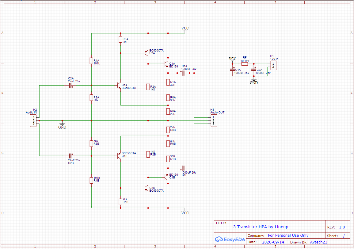
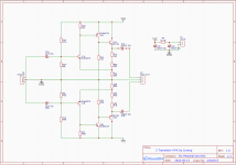
Here is an Amplifier using 3 transistors.
It has low distortion.
Gain is x4 which should be good for 32 Ohm headphones.
Power supply could be one LM317 set at 12 VDC.
All resistors can be 0.6 Watt.
Formula3HP
The latest version is in https://www.diyaudio.com/community/...p-amplifier-with-low-dist.359267/post-7055776
Attachments
Last edited:
Looks a nice simple single ended design, and I have almost all the required transistors!
missing the BC550C
Could I ask, what is the maximum input signal voltage?
Or put another way, when does clipping occur when the input signal is raised to 2.5Vp-p, for example?
Maybe 3dB of excess gain, for some situations. So perhaps room for a low level of NFB too, if desired
I'm going to find some BC550C, and build it!
Last edited:
> when does clipping occur when the input signal is raised
You do not have any volume control in your system?
Clipping point can be trivially figured from information in the first post.
You do not have any volume control in your system?
Clipping point can be trivially figured from information in the first post.
Looks quite simple to put together and I have everything available.
Might give it a go when I get the latest mess off my bench!
Might give it a go when I get the latest mess off my bench!
Maybe 3dB of excess gain, for some situations. So perhaps room for a low level of NFB too, if desired
Don't build it if you're leery of NFB -- it already has plenty.😉
The gain is set by the divider R1, R6, R8. If you want to cut 8 dBV of gain, just move the pick-off for U1's Emitter to the node between R1 and R6. There should be enough spare bias current that you won't have to fiddle U1's bias divider.
Nifty little design. Congrats lineup!

Cheers
Cheers Rick,
It isn't obvious to me that there is NFB, other than local degeneration. But I'm no expert.
I completely appreciate being made fo feel retarded, thank you!
PRR,
Funnily enough I do have a volume control, and even funnier, I usually design any amplifier to have the minimum excess gain, or just enough gain to do the job.
Is that wrong, when you know the outputs of your sources?
E.g. 32R phones dont need 8V p-p with 2V p-p signal input, unless the source is non standard output level or the phones are hideously insensitive.
But, Lineup circuit is elegant in its simplicity, and I cant wait to build, test, and modify. See how it performs in reality.
Last edited:
Sorry mondogenerator -- I surely didn't intend such an offense. It's late here and my old brain ..😱 I really should learn when to stop typing and go to sleep.
By the way, I appreciate - and agree with - your 'less wasted/discarded gain is better' philosophy. Used it a lot back in the pro sound days.
Best Regards
By the way, I appreciate - and agree with - your 'less wasted/discarded gain is better' philosophy. Used it a lot back in the pro sound days.
Best Regards
Rick,
No worries, I shouldnt have bitten.
It was early here, but the same problem. Still yawning!
No worries, I shouldnt have bitten.
It was early here, but the same problem. Still yawning!
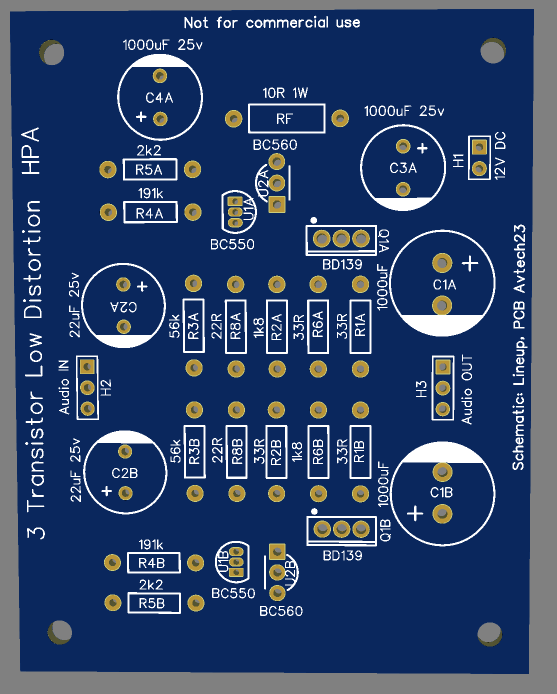
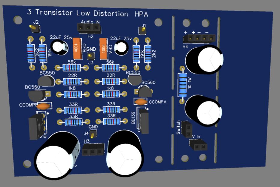
Lineup - I hope you don't mind but just for fun I threw together a board based on your design.
It's about 80*60mm (can easily be made smaller).
I intend on using a decently regulated PSU so I added a CRC filter (values to be finalised), instead of LM317. The CRC could also be CLC or just bypassed.
Can anyone see anything critically wrong or anything that stands out as might be problematic?
This layout is just single sided so the power supply is a little awkward being asymmetrical but I think it should be ok for a low power circuit.
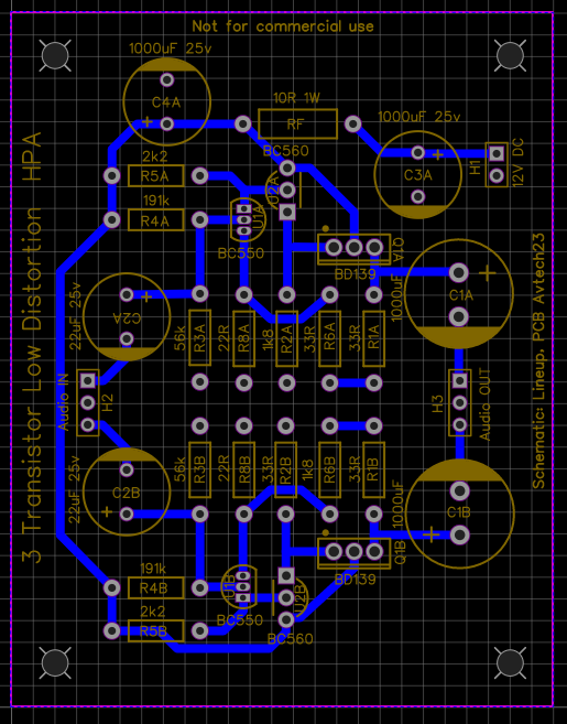
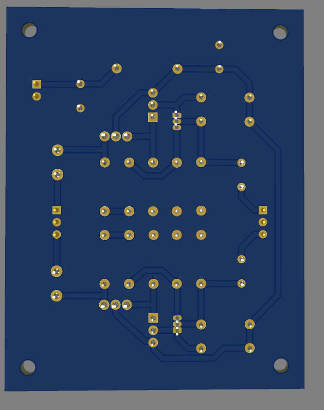
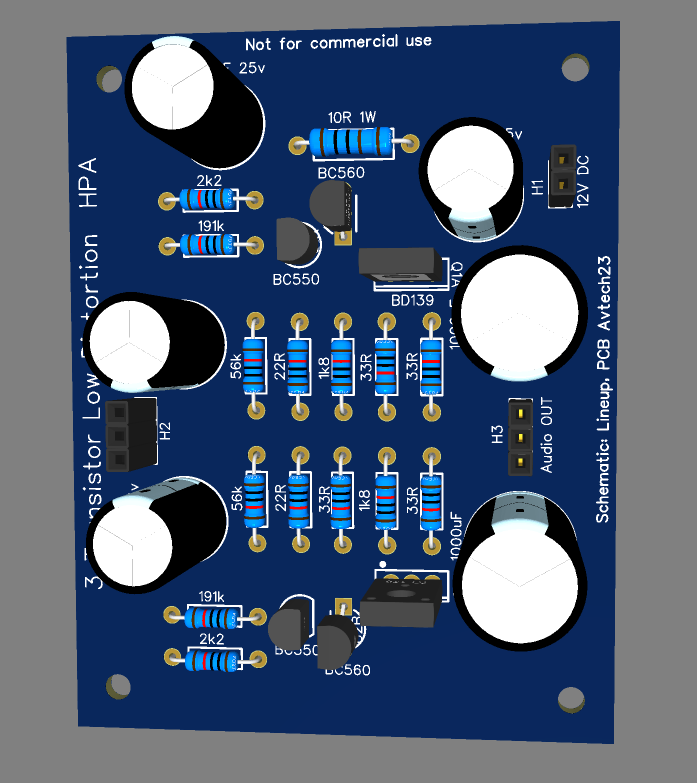
I've only designed a few boards so far, so I'm sure there are plenty of technique errors or misplaced components! 😱
Cheers.
It's about 80*60mm (can easily be made smaller).
I intend on using a decently regulated PSU so I added a CRC filter (values to be finalised), instead of LM317. The CRC could also be CLC or just bypassed.
Can anyone see anything critically wrong or anything that stands out as might be problematic?
This layout is just single sided so the power supply is a little awkward being asymmetrical but I think it should be ok for a low power circuit.
I've only designed a few boards so far, so I'm sure there are plenty of technique errors or misplaced components! 😱
Cheers.
Attachments


Hello,
The group of resistors R1, R6, R8 must be 1W.
Also Q1 mounted on a small radiator.
The consumption of the assembly is somewhere at 90-100mA.
The group of resistors R1, R6, R8 must be 1W.
Also Q1 mounted on a small radiator.
The consumption of the assembly is somewhere at 90-100mA.
Hi Marin,
Spice shows R1 and R6 at 288mW, R8 at 194mW, so 0.6w probably ok but maybe a bit warm.
The BD139 is showing around 300mW, so I would put a little heatsink on that for sure.
Clipping comes in around 550mV.
Spice shows R1 and R6 at 288mW, R8 at 194mW, so 0.6w probably ok but maybe a bit warm.
The BD139 is showing around 300mW, so I would put a little heatsink on that for sure.
Clipping comes in around 550mV.
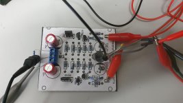
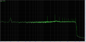
Oscillation seems to have been tamed using a 100pF compensation cap across the BC560. I tried 33pF but that wasn't sufficient - 100pF was next in stock.
I added 100n at the input to filter out a pulsing noise that I could hear, and now it is nice and quiet.
I used 600mW resistors and the 33 ohm are warm (60 deg) at 12 degrees ambient. The BD139 was about the same temperature without heatsinking.
Clipping is at 1.9v across a 47 ohm load resistor (I didn't have anything closer to 32 ohm for testing).
Sounds pretty good on the first test! I'll try to get some measurements done soon.
I'll try to get some measurements done soon.
Looking forward to these, thanks for posting your progress so far.
A beginner's question if I may? Does the oscillation come from the circuit as is or is it due to the layout or some other factor?
Looking forward to these, thanks for posting your progress so far.
A beginner's question if I may? Does the oscillation come from the circuit as is or is it due to the layout or some other factor?
Not sure to be honest. I'm certainly no layout expert so it is entirely possible I've committed some rookie error.
I'll try and do a phase margin plot on LTspice (when I remember how) and see if anything shows up there.
Here is the latest iteration of the board:
I'll try and do a phase margin plot on LTspice (when I remember how) and see if anything shows up there.
Here is the latest iteration of the board:
Attachments
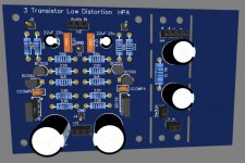
I made the above version of the board using 1W resistors for the 33R and 22R positions. (Note - I did not build the PSU filter, just the amp, so switching noise is possibly present).
I changed R4 and R3 to 180k and 51k respectively as these values are easier to obtain than the 191k. I simulated in LT and the change seemed to be suitable.
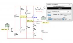
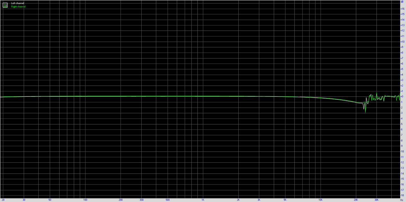
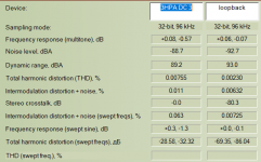
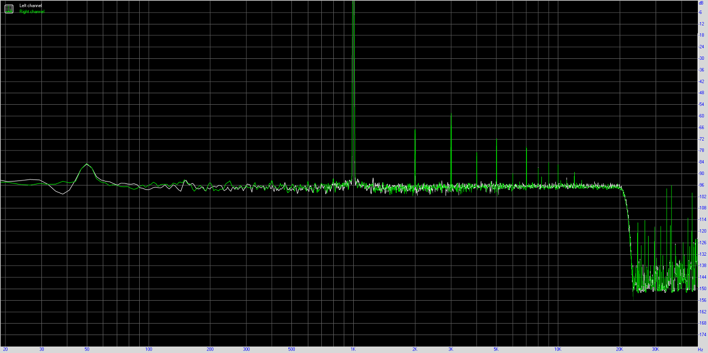
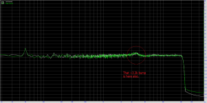
So here are the measurements into 47 Ohms, using a Focusrite Scarlett 2i4, laptop on battery:

THD:
Noise:
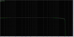
Frequency Response:
I changed R4 and R3 to 180k and 51k respectively as these values are easier to obtain than the 191k. I simulated in LT and the change seemed to be suitable.
So here are the measurements into 47 Ohms, using a Focusrite Scarlett 2i4, laptop on battery:
THD:
Noise:
Frequency Response:
Attachments

Last edited:
Ok I seem to have taken up half of this thread, so last one from me.
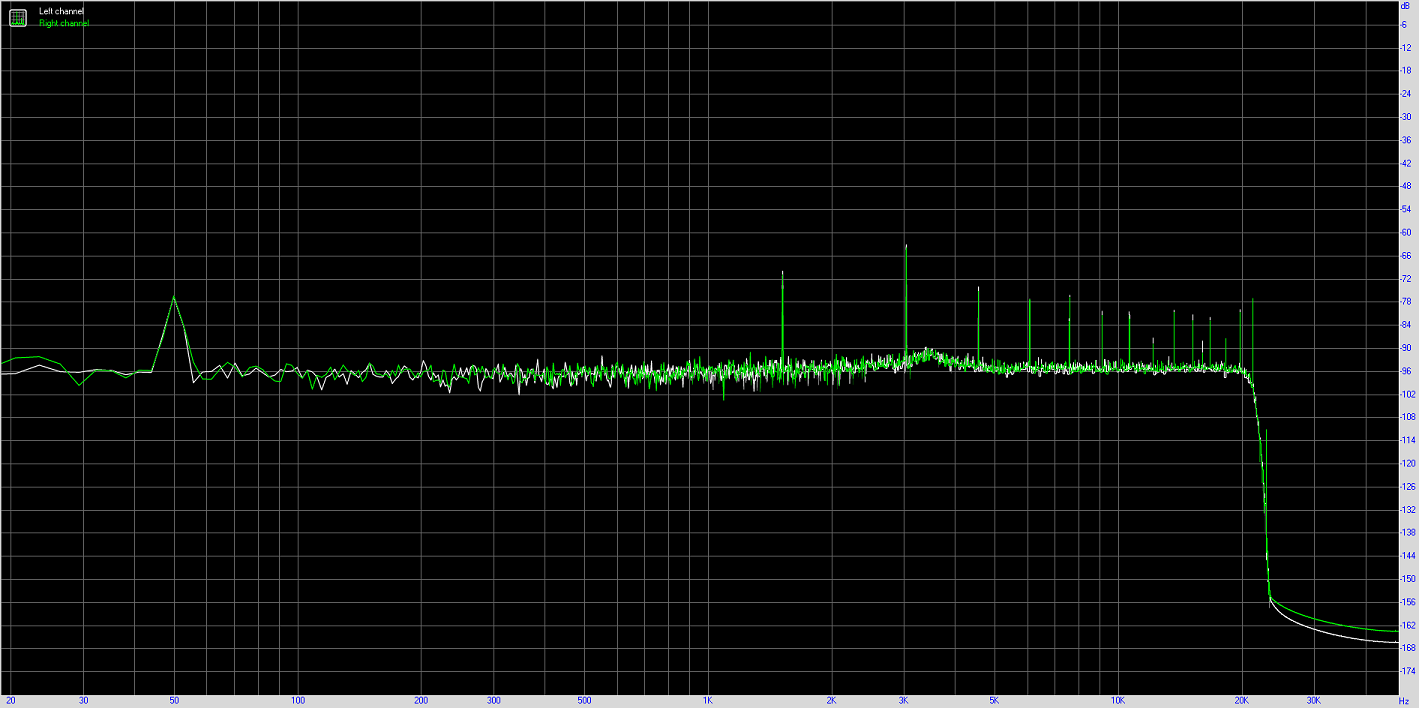
I've made some measurements with a CRC filter at the front of the power supply and got the following:
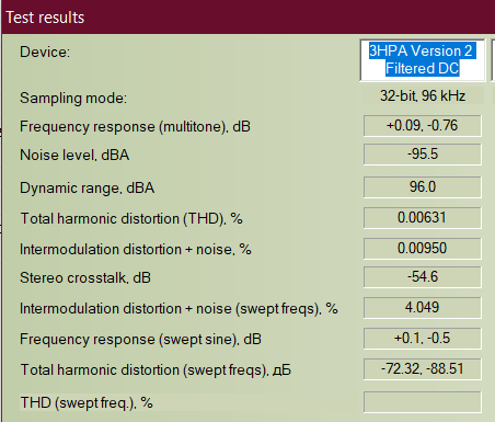
THD:
Noise:
Frequency Response:


I've made some measurements with a CRC filter at the front of the power supply and got the following:
THD:
Noise:
Frequency Response:
Attachments


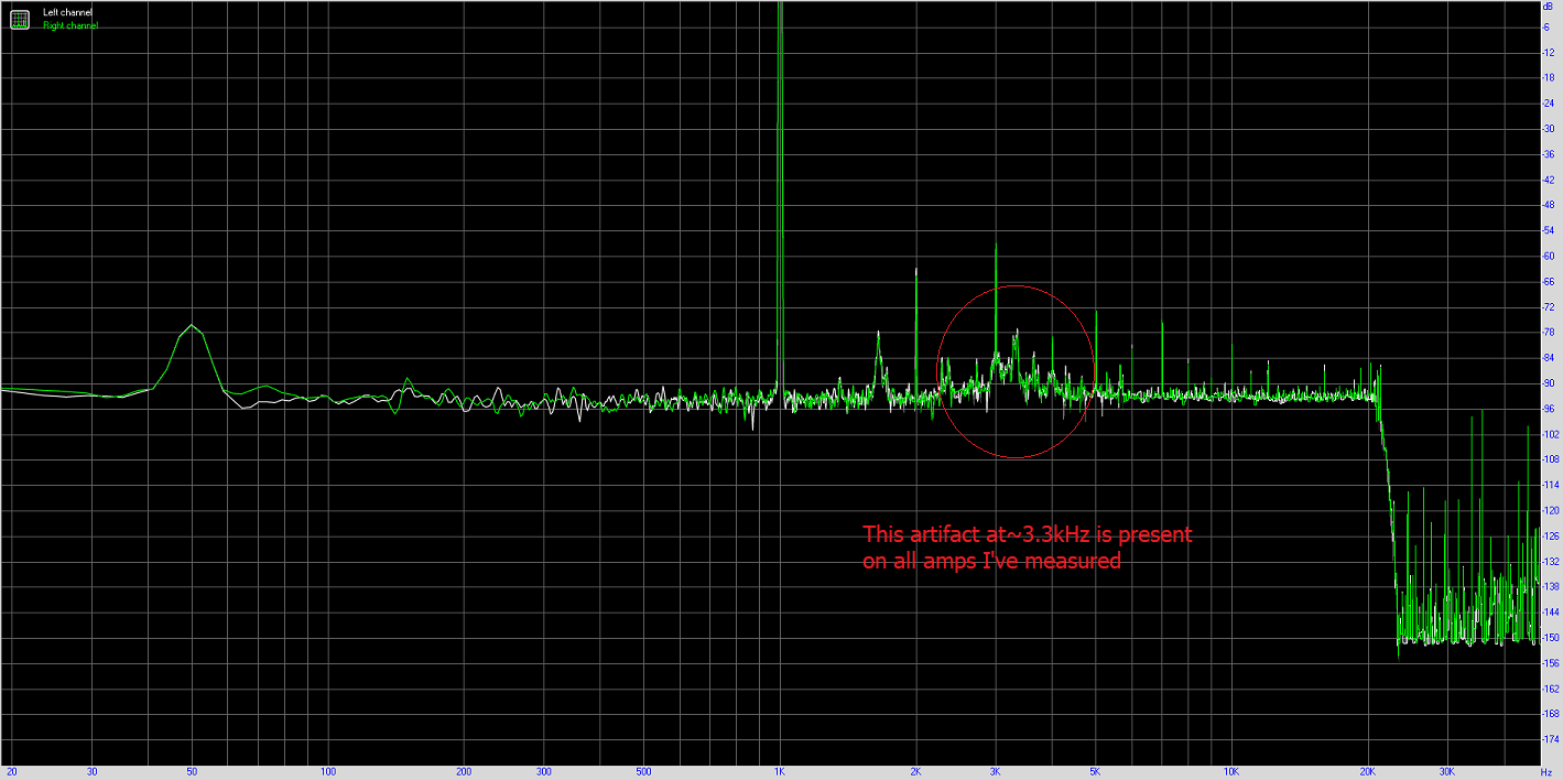
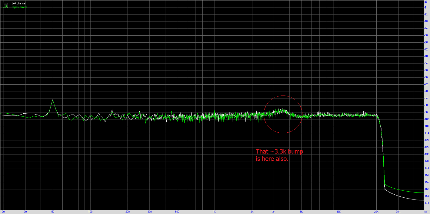
1. The 2-3 kHz artifact is probably ground loop noise. Make a cable that connects unbal-signal --> hot and unbal-ground --> cold, with shield connecting on the interface input side only. Then the balanced input should also be operating as such for once. (I mean, I could also be wrong and the noise may be inherent to the interface. Then it would also appear in a direct loopback.)
2. There is something amiss with the sample rate, the interface seems to run at 44.1 kHz only. If switching to ASIO in RMAA does not fix this, further investigation will be necessary (check interface control panel, check for updated drivers etc.).
3. Most any half-decent multimeter should be suitable for absolute level calibration, assuming it has something like a 20Vac range at least. Use 50-60 Hz if not True RMS.
Last edited:
Thanks for the tips.
I revisited the cables and they have been made correctly - twin shielded and screened audio cable with one wire from to signal - signal, one from gnd - gnd and shield connected to gnd only on the interface side.
Switching to ASIO makes the DUT clip so I need to look into this more.
I've had a look at the absolute level calibration and have a Fluke179 that is capable. I'll have a play with this to get consistency.
What voltages do you suggest for the testing?
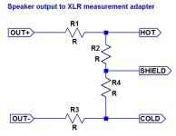
I am not actually convinced that this is correct. You should have the following input connector pinout:Thanks for the tips.
I revisited the cables and they have been made correctly - twin shielded and screened audio cable with one wire from to signal - signal, one from gnd - gnd and shield connected to gnd only on the interface side.
(XLR | TRS - at cable - at DUT output)
pin 1 | sleeve - cable shield - n/c
pin 2 | tip - cable hot - signal
pin 3 | ring - cable cold - gnd
Here's a matching attenuator topology as well:
This is useful for both BTL and SE outputs.
You may not need one if you have cables both for XLR (mic) and TRS (lone-level) input, as it looks like you have a wide variety of maximum input levels to choose from:
+3.5 dBu - XLR, no pad (there should be little degradation in input dynamic range when turning the gain up by up to about 20 dB)
+13.5 dBu - XLR, w/ pad
~+24 dBu - TRS, I'm guessing w/ pad
(Values taken from 2i4 1st gen manual, assuming this is the one you have.)
You may have had the output turned down digitally (maybe the software volumee control exposed in the OS is driver-level attenuation only). Turn down the 2i4's MONITOR control to reach previous levels. Turning up volume in Windows should bring non-ASIO levels up.Switching to ASIO makes the DUT clip so I need to look into this more.
1 Vrms (XLR no pad) and 2 Vrms (XLR w/ pad) would be pretty standard, I suppose.I've had a look at the absolute level calibration and have a Fluke179 that is capable. I'll have a play with this to get consistency.
What voltages do you suggest for the testing?
4 Vrms would be of interest with a 300 ohm load (TRS input should still do that w/o pad)
400 mV may be of interest with e.g. a 32 ohm load in particular (I presume distortion with 300 ohms would be well-described by intercept points at these levels, i.e. should agree well with levels extrapolated from 1 Vrms).
Attachments
- Home
- Amplifiers
- Headphone Systems
- 3 Transistor HP Amplifier with low dist