Hitachi lateral mosfet datasheet had this circuit.
Maplin copied it and loads in the 1980's.
i rehashed it few years back using mpsa42/92 and profusion lateral mosfets.

Maplin copied it and loads in the 1980's.
i rehashed it few years back using mpsa42/92 and profusion lateral mosfets.
My build
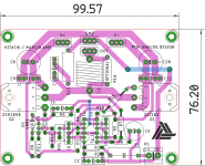
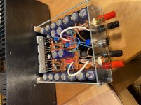
So, I (almost) finalised my build. The back plate I still a mock-up while I wait for the remaining parts.
The idea of the build was to use a surplus heat sink and four 19.5V/ 90W Laptop SMPSs I could salvage.
When I saw Juma's post #180 I found that this was the schematic I wanted to try.
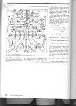
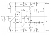
Bias I kept at 700mA, heatsink goes to 51°C.
Attached also the final configuration I chose.
R9 is 10k to yield a gain of x10.
As per Anatoly's suggestion I changed C4 to terminate at the collector of Q4 instead of at the output.
In the original config I found it hard to keep the circuit from oscillating.
J1/J2 are SMD, mounted closely together on the same small piece of PCB, dropping the source resistor R6 (schematic of post # 180).
C2 is 220uF which gives smoother turn-on/off thumps with the SMPS.
D1 I replaced by a TL431 plus resistor & pot to be able to tune the bias to the capacity of the heat sink.
Also I inserted an orange LED between the collector of Q3 and the negative voltage supply.
Firstly, because it shines orange. But I also found it useful for debugging while tampering with the circuit as it indicates that there is current through J1/J2/Q3.
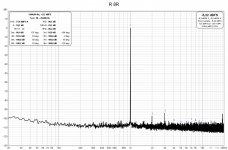
With 1kHz sine into 8 Ohm dummy load @ 8Vpp I measure H2 -96dB and H3 -94dB as shown in the attached graph (Behringer UCA202, REW).
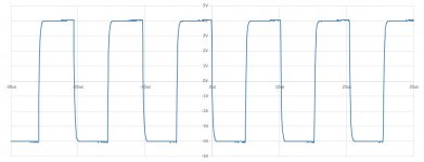
100kHz square wave 8 Vpp into 8 Ohm I also attached.
The sound of the amp I find quite authoritative. I run it in my study fed from a Topping D10 (no preamp) into Linn Index speakers. The bass isn't loud or booming, but surely commanding.
So, I (almost) finalised my build. The back plate I still a mock-up while I wait for the remaining parts.
The idea of the build was to use a surplus heat sink and four 19.5V/ 90W Laptop SMPSs I could salvage.
When I saw Juma's post #180 I found that this was the schematic I wanted to try.
Bias I kept at 700mA, heatsink goes to 51°C.
Attached also the final configuration I chose.
R9 is 10k to yield a gain of x10.
As per Anatoly's suggestion I changed C4 to terminate at the collector of Q4 instead of at the output.
In the original config I found it hard to keep the circuit from oscillating.
J1/J2 are SMD, mounted closely together on the same small piece of PCB, dropping the source resistor R6 (schematic of post # 180).
C2 is 220uF which gives smoother turn-on/off thumps with the SMPS.
D1 I replaced by a TL431 plus resistor & pot to be able to tune the bias to the capacity of the heat sink.
Also I inserted an orange LED between the collector of Q3 and the negative voltage supply.
Firstly, because it shines orange. But I also found it useful for debugging while tampering with the circuit as it indicates that there is current through J1/J2/Q3.
With 1kHz sine into 8 Ohm dummy load @ 8Vpp I measure H2 -96dB and H3 -94dB as shown in the attached graph (Behringer UCA202, REW).
100kHz square wave 8 Vpp into 8 Ohm I also attached.
The sound of the amp I find quite authoritative. I run it in my study fed from a Topping D10 (no preamp) into Linn Index speakers. The bass isn't loud or booming, but surely commanding.
Attachments
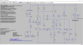

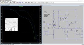
Phase Margin
Coming back to C4, I tried to rationalise how my prototype oscillated in the original config and didn't when I put C4 between R8/R9/C3 on the one side and the collector of Q4 on the other.
I followed the notions Simon Bramble put forward for loop analysis and arrived at the attached results.
The green curves show loop gain and phase for the configuration in post #180 and the blue lines when considering Anatoly's suggestion.
If I did this correctly the curves show that at a phase of -180° the original schematic still has positive loop gain suggesting instability. Anatoly's version has a minimum loop phase of -125° far away from -180°.
I appreciate that this is a simulation and the reality will be quite different especially at the frequencies in question. But did I do the analysis roughly right?
Attachments
D1 I replaced by a TL431 plus resistor & pot to be able to tune the bias to the capacity of the heat sink.
You need these to run the sim.
Attachments
I took another look - I made an error in assessing the output impedance. I neglected to ground the input. With the input grounded, it looks reasonable.
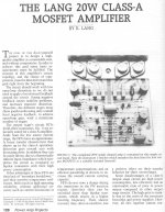
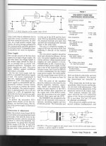
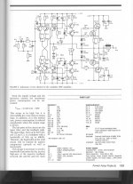
We should try well tested projects mostly. Class A amps need very good dc filrering with capacitance more than 40.000uF , dual rail dc power supplies and small negative feedback. There it is a project from an electronics magazine. It has 4 lateral mosfet per channel-2SK133/134/135 and 2SJ48/49/50 with a 2A quiescent current for pure class A operation. It needs huge heat sinks but its sound performance is outstanding.Have a look!!
Attachments
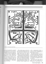

Very simple amp design. Here is the layout i came up with KSA992/KSC1845🙂
Very nice layout Prasi and super simple to build. I would like to build this amp as I have 2 pairs of matched original Hitachi 1058/162 lateral mosfets. Please share pair of boards or gerber files.
Thanks
The Layout I have only for home brew type. No gerber files. In case if you was asking for that.
At first glance it is very similar to this amp. It has (I have) the layout for the plastic type 2SJ/2SK power mosfets.🙂
There are some critical differencies. There is no RF filter rejection at the output and no quiescent current adjust. What for is the pot at both supply rails? here is the pdf
Attachments
Reason I wrote similar.
The existing PCB layout easily can be modified and you end up with parts you can still source in the market. Those metal case Mosfets are very rare and be aware for fakes Ebay stuff.
Maybe you can get some BUZ types.
I do not want to build the amp. It was a time when I was interested. No longer.
The existing PCB layout easily can be modified and you end up with parts you can still source in the market. Those metal case Mosfets are very rare and be aware for fakes Ebay stuff.
Maybe you can get some BUZ types.
I do not want to build the amp. It was a time when I was interested. No longer.
Zobel filter at the output is not needed, the amp is stable without it.There are some critical differencies. There is no RF filter rejection at the output and no quiescent current adjust. What for is the pot at both supply rails?...
Adjustment of quiescent current is accomplished with pots in sources of 2sk30 JFETs - they act as CCSs and you adjust them alternatively (like in F5/F6 amp) to set the quiescent current and symmetry (0V DC offset at the output).
Also, in K.D.Lang amp, there is only 2mA through D1/D2 and 0.6mA through D3/D4 (which makes all these zener diodes too noisy) etc...
Last edited:
i have built that amplifier and I can assure you that it plays just fantastic, no noise and stable operation with 2A quiescent current. if you match both BC550 and 560, the offset voltage is smaller than 10mV.
One quick question I have built Maplin amp using Prasi provided gerbers and the amp is up and running. I checked the bias across R11 (100R) resistor and using the trimmer set to 400mV with the offset being self around 5-7mV. I am using a 22vac trafo so getting around 34.5vdc rails. Want to know whats the right bias across this 100R resistor for optimal. I have used a small heat sink like 120/100/50mm and it gets very hot too fast. Hence planning to move it to 300/150/83 after the completion.
Thanks
Thanks
If I remember right the bias current should be 100mA.
So put multi-meter on current range across fuse holder (after fuse taken out.)
With 100mA bias the heat sink soaks up 3 watts even with no signal.
So put multi-meter on current range across fuse holder (after fuse taken out.)
With 100mA bias the heat sink soaks up 3 watts even with no signal.
- Home
- Amplifiers
- Pass Labs
- 25W Class A amp with Lateral MOSFETs