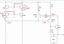
Hi, here is the schematic on test:

EDIT: I corrected the schematic
I omitted the output stage because of space, and because it is not really important to know so much about it: it's only a classic emitter-follower output.
Straight to the problem: distortions created by VAS current limiter. The transistors are Q15 and Q18.
That is strange because this should not affect the VAS, current limiting should only guarantee a static current and not create distortions. Yet it seems that with the spectrum analyzer (in the real model) its presence and absence make the difference between having so much distortion and having little.
I'll explain:
- Raising the biasing current, the situation does not change.
- Both with and without the current limiter on the VAS, transistors Q14 and Q16 always have 5.5mA of through current.
- By changing the output stage, changing it in many different ways, the situation does not change.
- No load, no distortion register at the amplifier output. But with even 8 ohms of load, and high output transistor polarization, if the current limiters are present, the distortion is 0.85%, while without them it is 0.01%.
You say: if the current is the same with and without, why not simply removing it?
I say: the current passing is highly variable based on the beta of the transistor, and also because the current varies greatly based on the increase in temperature.
What I have done wrong in this configuration?
Last edited:
Q14 and Q16 look like the first part of a EF driver.
The current they deliver tot he output goes through the current limit resistor. This will effectively "turn the VAS current limit on" - even though the VAS current itself is controlled.
Connect the collectors of Q14 / 16 tot he appropriate rails and the CAS current limit will work as you expect.
The current they deliver tot he output goes through the current limit resistor. This will effectively "turn the VAS current limit on" - even though the VAS current itself is controlled.
Connect the collectors of Q14 / 16 tot he appropriate rails and the CAS current limit will work as you expect.
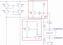
Hi Northumber, your schematic has a bunch of problems:
1- Transistor sense: On both input stages, PNP should be NPNs, and NPNs should be PNPs.
2- 2nd diff pair current mirror: On the second diff-pair (the middle one), you are taking the output of the wrong side of the mirror. Unless, you are really wanting to take it from the mirror input to make a signal dependent current source out of Q11.
3- VAS Bias current: Assuming Q11 base is re-wired to the output of the current mirror, how are you biasing the VAS stage, i.e. how are you defining the standing current.
Best, Sandro
Q14 and Q16 look like the first part of a EF driver.
The current they deliver tot he output goes through the current limit resistor. This will effectively "turn the VAS current limit on" - even though the VAS current itself is controlled.
Connect the collectors of Q14 / 16 tot he appropriate rails and the CAS current limit will work as you expect.
No, that are not the first part of the driver of the output stage, but litterally the VAS stage. It is the CFP configuration of the emitter-follower VAS. Changing the VAS to emitter-follower does not change the situation, there are always distortions.

Hi Northumber, your schematic has a bunch of problems:
1- Transistor sense: On both input stages, PNP should be NPNs, and NPNs should be PNPs.
2- 2nd diff pair current mirror: On the second diff-pair (the middle one), you are taking the output of the wrong side of the mirror. Unless, you are really wanting to take it from the mirror input to make a signal dependent current source out of Q11.
3- VAS Bias current: Assuming Q11 base is re-wired to the output of the current mirror, how are you biasing the VAS stage, i.e. how are you defining the standing current.
Best, Sandro
Yes, you are correct on the first two points, I drawed the schematic rapidly with a copy and paste and I didn't notice, because I was interested in the VAS stage. Excuse me for that.
In what sense biasing the VAS stage? I tried to put and varying resistor on emitters of current mirror, but the situation is the same.
EDIT: anyway, input stage current -> varying 47 ohm resistor or varying 2.2k resistor
Last edited:
Well, I think your problem is that you don't have explicit circuitry to set the standing current of Q11, Q14, Q17 and Q16. If you cannot write a formula that shows that the current of these transistors should be X,Y,Z mA. Then you are not setting the bias current right. I would consider fixing this first.
Best, Sandro
Best, Sandro
Hi
The whole input stage is drawn wrong, including the Wilson current mirrors. For the PNP input stage, emitters tie together and the collectors go to the mirror, which should be comprised of NPNs with emitters tied to the rail. Similarly, the NPN diff amp should have emitters tied together and work into a PNP mirror with its emitters to the rail.
As far as the current clamps go, they look pretty standard. I found it useful to place a resistor between the clamp transistor collector and the base of the VAS device.
It is questionable whether the VAS current will be stable or even predictable in a reliable way, as others point out above. There has been much discussion about this in the reference books and on this forum. many use Bob Cordell's "helper transistor" style current mirror so there will be one mirror at least with a voltage reference built in. An alternative is to replace one mirror with simple resistive loads.
Hi
The whole input stage is drawn wrong, including the Wilson current mirrors. For the PNP input stage, emitters tie together and the collectors go to the mirror, which should be comprised of NPNs with emitters tied to the rail. Similarly, the NPN diff amp should have emitters tied together and work into a PNP mirror with its emitters to the rail.
As far as the current clamps go, they look pretty standard. I found it useful to place a resistor between the clamp transistor collector and the base of the VAS device.
It is questionable whether the VAS current will be stable or even predictable in a reliable way, as others point out above. There has been much discussion about this in the reference books and on this forum. many use Bob Cordell's "helper transistor" style current mirror so there will be one mirror at least with a voltage reference built in. An alternative is to replace one mirror with simple resistive loads.
Yes, I know that is wrong, as I already wrote along the post (I don't know if you read the answers), I drew it in a hurry, using copy paste, without realizing it.
There has to be some element that sets the VAS bias to something less than half the limit current, ie < 0.65/47/2 < 7mA but there is no such feature in bipolar VAS circuits like this one, assuming the other problems are fixed. Normally the LTP current is applied to resistors and not current mirrors, and that creates a voltage, minus the VAS Vbe, across VAS emitter resistors then defines the VAS current. Alternately the VAS is itself a current mirror so that the VAS current is defined as some factor X the LTP current. This is one reason that bipolar VAS circuits are not more popular. The VAS bias current is simply undefined, ie unpredictable.
BTW, bipolar VAS circuits are like symmetrical panel layouts. The symmetry appeals to certain peoples but they fail to deliver superior results.
BTW, bipolar VAS circuits are like symmetrical panel layouts. The symmetry appeals to certain peoples but they fail to deliver superior results.
Last edited:
You need a resistor from base Q11 to base Q17 to provide bias current for VAS stages. The current mirrors subtract each other.
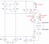
I corrected the schematic in the first post, can now you explain me how to resolve this situation?
What is the circuit to apply to this to set the bias current for the VAS?
What is the circuit to apply to this to set the bias current for the VAS?
May be your correct input circuit like this, Q6,Q8 make a 1.2V to Q11 base and Q15 base may be around 0.6V, Q15 may be partial kick in.
For VAS current limiter, no need base resistor, if remove R9, Q15 maybe full kick in.
to keep your input circuit, you can remove both VAS current limiter transistor, just use a 10 ohm low wattage fusible resistor between Q14 output to bias ciucuit and make the over current protection.
For VAS current limiter, no need base resistor, if remove R9, Q15 maybe full kick in.
to keep your input circuit, you can remove both VAS current limiter transistor, just use a 10 ohm low wattage fusible resistor between Q14 output to bias ciucuit and make the over current protection.
Attachments
Does the original circuit 4-transistor current mirror not bottom out trying to drive the VAS?
With an EF VAS the extra drive voltage required by 2 Vbe drops allows a higher-drop-out current mirror, that VAS topology doesn't I suspect...
I see no Miller cap in that VAS to linearize it, so it ought to be unstable and non-linear from the get-go. The Miller cap has an important role as local feedback around the IS/VAS combination. Otherwise you have a simple common-emitter stage with almost no degeneration - pretty non-linear.
for your new circuit, try remove Q15 and test Q11 base voltage if it is 1.2V. If Q11 base voltageis 1.2V, you can change current limiter Q15 base kick in voltage control by a resistor divider.
With and without the Q15, voltage between supply rail and Q11 base is 0.7V
Does the original circuit 4-transistor current mirror not bottom out trying to drive the VAS?
With an EF VAS the extra drive voltage required by 2 Vbe drops allows a higher-drop-out current mirror, that VAS topology doesn't I suspect...
I see no Miller cap in that VAS to linearize it, so it ought to be unstable and non-linear from the get-go. The Miller cap has an important role as local feedback around the IS/VAS combination. Otherwise you have a simple common-emitter stage with almost no degeneration - pretty non-linear.
I simply omitted the miller cap to simplify, but it is obviously present in the real model.
With and without the Q15, voltage between supply rail and Q11 base is 0.7V
your measure result, Q15 current flow is not equal the total current flow of Q11 and Q14, please double check the circuit.
Attachments
your measure result, Q15 current flow is not equal the total current flow of Q11 and Q14, please double check the circuit.
All the voltages you have marked in the various points are correct: 0.7, 0.6 and 0.1.
All the voltages you have marked in the various points are correct: 0.7, 0.6 and 0.1.
"Both with and without the current limiter on the VAS, transistors Q14 and Q16 always have 5.5mA of through current."
you said Q14 current flow is 5.5mA, this current will be not correct
you said Q14 current flow is 5.5mA, this current will be not correct
I'm doing it wrong or the current passing through R6 should be 6mA and not 2mA?
- Home
- Amplifiers
- Solid State
- Problems with VAS current limiting