Perhaps the design team simply tried a bunch of random ideas in the simulator, and chose the one(s) which gave the most pleasing simulation output. In the same vein as the hypothesis that it is possible to play the piano, without actually knowing how its internal mechanisms operate; and also without even knowing how to read sheet music.
I would be ok with that.
I guess it depends how easy it is to get perfection. If it’s easily improved then may as well improve it. It probably won’t be an audible improvement but I understand these thing can help you just enjoy listening to music better. I don’t want to be thinking about such things when I listen to music assuming it irritates you wondering about it.
I guess it depends how easy it is to get perfection. If it’s easily improved then may as well improve it. It probably won’t be an audible improvement but I understand these thing can help you just enjoy listening to music better. I don’t want to be thinking about such things when I listen to music assuming it irritates you wondering about it.
If the amplifier is well-approximated by a second order linear system, theoreticians have worked out LOTS of this_versus_that relationships. Google finds them but it takes more than 15 minutes (and less than 90 minutes). Here is a plot of one such relationship:
Overshoot of square wave response
versus
Phase Margin
You will notice that SOME overshoot is expected in MOST amplifiers.
_
Overshoot of square wave response
versus
Phase Margin
You will notice that SOME overshoot is expected in MOST amplifiers.
_
Attachments
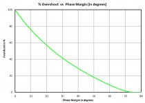
Yeah, and it gives the perspective I didn't have. The overshoot in my picture is about 1/2 of 1%, which appears to be pretty minor.
(Funny enough, the chart also makes an accurate prediction with the CFA, which has a 69º phase margin. It doesn't do quite as well with the Hitachi topology which shows no overshoot but has a similar 68º phase margin.)
(Funny enough, the chart also makes an accurate prediction with the CFA, which has a 69º phase margin. It doesn't do quite as well with the Hitachi topology which shows no overshoot but has a similar 68º phase margin.)
Nice graph. Hadn’t see that one before.
http://eas.uccs.edu/~cwang/ECE5955_F2015/PowerElectronics_f2015/ch9/Sect9-4-2.pdf
Oh, neat, and that one does indeed predict oscillation:

Would you be able to post the schematic showing the location of the nodes in the plot and the Voltage sources used?
This would be very helpful understanding the evaluation of stability and compensation in ltspice. Thus far I have only looked at the output node with a Vsource at the input, AC 1. I saw in a later schematic there was a Vsource in the feedback loop with value AC 1.
Once there is the desired bode plot, what general criteria need to be met? (I'm a third year EE student, not PhD) I've read many different sources and get lost somewhat in the tangents.
Yes, to get open-loop gain you need to break the loop and inject the AC in the feedback loop (through V1 in the attached .asc). Then you plot the nodes on either side of the injected AC.
I've attached the .asc file for this front-end:

Run an AC analysis.
Plot V(FB)/V(NFB).
Create a cursor and move it to the right until the gain reaches 0dB. Look in the cursor window and the reported phase is your phase margin.
Keep moving the cursor until the phase reaches 0º. Note the gain reading (in dB): the absolute value of that is your gain margin.
Give a holler if you get stuck.
Cheers,
Jeff.
I've attached the .asc file for this front-end:
Run an AC analysis.
Plot V(FB)/V(NFB).
Create a cursor and move it to the right until the gain reaches 0dB. Look in the cursor window and the reported phase is your phase margin.
Keep moving the cursor until the phase reaches 0º. Note the gain reading (in dB): the absolute value of that is your gain margin.
Give a holler if you get stuck.
Cheers,
Jeff.
Attachments
Thanks for the reply!
The plot for the design I'm working away at and have acquired most of the transistors for has a very similar set of curves. This thread has been very helpful. All the femto nuggets of info along the way are appreciated.
The plot for the design I'm working away at and have acquired most of the transistors for has a very similar set of curves. This thread has been very helpful. All the femto nuggets of info along the way are appreciated.
One of my previous compensation schemes for the Hitachi topology required a lot of current through the LTP, resulting in about 400mA dissipation in the cascodes. I didn't want to run TO92s that hot so I replaced the KSA992s with KSA1381s.
The current compensation scheme has them down to a more manageable 220mA, so I could go back to KSA992s. Should I, or are the TO126 KSA1381s just as good for this anyway?
Thanks,
Jeff.
The current compensation scheme has them down to a more manageable 220mA, so I could go back to KSA992s. Should I, or are the TO126 KSA1381s just as good for this anyway?
Thanks,
Jeff.
The design isn't done once the simming is finished. There will be room and perhaps need for fine tuning later.
Time to move on, as they say... 🙂
Time to move on, as they say... 🙂
Does any one know if theirs a reason not to use IRF510/9510 as JFET cascodes rather than BJT's?
Higher parts-count (once you stick the gate resistors in).
Higher parts-cost (for manufacturers anyway).
Those may explain why you don't often see MOSFETs there. Or, maybe you don't often see it because it doesn't work well?
I know, fat lot of help I am....
Higher parts-cost (for manufacturers anyway).
Those may explain why you don't often see MOSFETs there. Or, maybe you don't often see it because it doesn't work well?
I know, fat lot of help I am....
- Home
- Amplifiers
- Pass Labs
- JamJar: an HPA-1-inspired power amp