> Dont' I have to consider voltage sweep in my computations?
The input voltage to a *grounded* Emitter is about 20mV for 20% THD.
You seem to have figured Rin of Q8 as 2.4k. (Seems a wee bit high.) If R9 were much higher than 2k you would have maximum *current* transfer and could arrive at a lower parts count; however you also get lower bandwidth and slow recovery after clipping. (I went this way in my post #19 quickie.) If R9 is much much lower than 2k you have solid drive to Q8 but maybe more current in Q10 than you "need", so high Q10 base current and increased DC error. Your 680:2400 ratio is reasonable pencil-guess.
> fixing the behaviour of each one before proceding with the next one?
Again: "Designing an amplifier is a recursive operation. ..., you always progress in spiral form...."
The other (and frankly more profitable) path is Plagiarize-Plagiarize-Plagiarize!! Study ALL amps you can find. See why they work. Build some rules-of-thumb about topology and working current. In my taxonomy your assignment seems to seek what I would call "Early Bipolar Fisher". Because I had access to factory-reject Fisher amp modules, about the time Fisher moved to diff-in and bipolar supply. Everybody was going this way; _I_ just got my education on Fishers. Mostly more complex than your assignment asks for, but seeing the basics is part of your education.
Unfortunately I still don't understand.
Btw I thought that the input acted as the VAS: aren't them both CE amplifiers?
Btw I thought that the input acted as the VAS: aren't them both CE amplifiers?
Unfortunately I still don't understand.
Btw I thought that the input acted as the VAS: aren't them both CE amplifiers?
I thought we were talking about a 3 stage amp in this thread? Input differential pair, VAS, OS.
The output of the input stage is a current, not a voltage, in other words the input stage is transconductance amp (voltage in, current out), the VAS is transimpedance (current in, voltage out).
How can you say that?
What about the OS? Voltage in and voltage out?
At all but the lowest frequencies the transimpedance of the VAS is determined by the Miller compensation capacitor, not the transistors, since it sets up local feedback around the VAS transistor(s).
What does this fact imply?
The transimpedance of the VAS at DC is affected mainly by its loading, which is why its typically given a constant current source load (very high impedance).
I don't get it.
negative loop gain?
Hi all
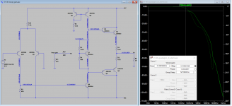
I was dimensioning the CE capacitor. To do that I was looking at some formulas seen in class. The formula (freq_C=1/(2*pi*Req*C)) involves the knowledge of the loop gain (open loop gain*beta). It appears to be negative in my schematic. What does it mean? Is something wrong? In a different exercise done in class I got a positive number: I though positive numbers were to be expected.
Hi all
I was dimensioning the CE capacitor. To do that I was looking at some formulas seen in class. The formula (freq_C=1/(2*pi*Req*C)) involves the knowledge of the loop gain (open loop gain*beta). It appears to be negative in my schematic. What does it mean? Is something wrong? In a different exercise done in class I got a positive number: I though positive numbers were to be expected.
Attachments
Last edited:
Hi Luka, are you still seeking help on this? Also, is there a noise spec?
More importantly, what about idle power consumption?
Best, Sandro
More importantly, what about idle power consumption?
Best, Sandro
Last edited:
> appears to be negative
I would worry more about why you have 14V DC on the output. That can't be good for the speaker. And it implies the active gain is jammed-up, which would explain no-gain.
The NFB loop normally works to set output DC near input DC.
Ah, you broke the NFB loop. Yes, that can work on low gain amps but not this one. There is some technique to keep DC NFB happening but cut audio NFB.
Alternatively close the loop and measure the AC *across* the input bases, compared to output AC.
When the feedback is on place only 25mV DC offset appears at the output.
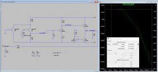
RF1 and RF2 are attached to the the output thanks to "vo" label. After I've seen peaking in my circuit with feedback I decided to choose a capacitor for Q8. To choose its size I grounged the negative input detaching the feedback in order to get the loop gain using an ac analysis. I was following this path: allaboutcircuits.com/technical-articles/… After that I can find the frequency of the pole of the added capacitor. After that I can find the size of the capacitor with the formula I mentioned.
RF1 and RF2 are attached to the the output thanks to "vo" label. After I've seen peaking in my circuit with feedback I decided to choose a capacitor for Q8. To choose its size I grounged the negative input detaching the feedback in order to get the loop gain using an ac analysis. I was following this path: allaboutcircuits.com/technical-articles/… After that I can find the frequency of the pole of the added capacitor. After that I can find the size of the capacitor with the formula I mentioned.
Attachments
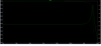
If you want an open-loop gain plot, just add a very large inductor in series with RF2, like 1MEG or even 1G. Alternatively, look up "Tian probe".
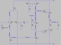
The output stage is likely to work better if you add a resistor between Q3 and Q4 emitters (try 330 ohms for starters) and tweak bias as needed. As-is, you should find considerable cross-conduction when crossing over at high frequencies.
The output stage is likely to work better if you add a resistor between Q3 and Q4 emitters (try 330 ohms for starters) and tweak bias as needed. As-is, you should find considerable cross-conduction when crossing over at high frequencies.
If you want an open-loop gain plot, just add a very large inductor in series with RF2, like 1MEG or even 1G. Alternatively, look up "Tian probe".
The output stage is likely to work better if you add a resistor between Q3 and Q4 emitters (try 330 ohms for starters) and tweak bias as needed. As-is, you should find considerable cross-conduction when crossing over at high frequencies.
Why cross-conduction over high freq should appear?
The bias I need to twek is related to the Vbe multiplier right? More than 10mA quiescent current in R1 I have to seek, right?
Cheers
Turning an output transistor off requires depleting a not-insignificant base charge (up to 1-3 nF). Depending on driver stage current, that takes its time. Even worse, at present that base charge has to be drained purely by the output transistor's own base current. So you get a certain time interval where a transistor should actually be off but isn't, while the other half of the output stage has already started to conduct.Why cross-conduction over high freq should appear?
Bob Cordell's book goes into some depth on this particular topic. It is also related to the discussion of Darlington turn-off in general.
There is at least one (old) amplifier design known to be prone to burning up when confronted with a full-power 20 kHz sine.
That sounds like something Master Yoda would say. 😉 But yes, just that. Probably rather more than less, as sluggish as these output transistors are.The bias I need to twek is related to the Vbe multiplier right? More than 10mA quiescent current in R1 I have to seek, right?
Last edited:
- Home
- Amplifiers
- Solid State
- Three stages amplifier college project help