Different gate stopper resistors compensate to some degree differences in input capacitance but this is academic at best because there are a lot of different characteristics that have to be looked at such as Rds.
Toshiba seems to make the best complementary mosfet devices, the Hitachi's tend to suffer from low trans-conductance.
The IR9240 for example has a anomaly compared to its complement for example and it is well documented.
As always any design has a lot of compromises but the best designs reduce the number you have to make. The correct topology and devices for the application has to be chosen.
Jam
Speaking of laterals not being terribly complementary, you'll notice that my gate stoppers are unbalanced to even out the phase response (due to unequal Ciss). But I note that many of the other circuits don't do this.
Unnecessary? Bad idea? Good idea?
Seems we read the same application note ..😉
... In post 32 I would cascode the VAS mosfet....
Like so?
(I also tried it with another 2SK2013 biased with the LTP cascode's bias circuit. That showed slightly worse distortion.)
Cheers,
Jeff.
Attachments
I think he means cascoding at drain not source.
If necessary use voltage dividing network or plain voltage source at gate of mosfet/jfet/bipolar cascode to ensure correct operation of cascode.
If necessary use voltage dividing network or plain voltage source at gate of mosfet/jfet/bipolar cascode to ensure correct operation of cascode.
Last edited:
Assuming you're using a bipolar cascode just use half the rail voltage at the base of the bipolar as a rough starting point.
I'm not entirely sure what I'm trying to accomplish with the cascode (pointers appreciated), but here are the THD results I get at 120W:
No cascode 0.064
DN2540 below 0.063
DN2540 above 0.066
2SK2013 below 0.063
2SK2013 above 0.070
The two below are a (slight) improvement, while the two above measure worse than the baseline. But again, I'm not entirely sure what I'm looking for so maybe it's just not encoded in to the THD?
(They do have different sweet spots for the degeneration, which I didn't think to include in my previous reply which accounts for thinking the 2SK2013 was worse than the DN2540.)
Cheers,
Jeff.
The cascode helps linearise capacitances.
It should result in lower distortion at higher frequencies say above 10kHz and at higher voltage swings eg if the rails are 30V then at voltage swings above 20V.
It should result in lower distortion at higher frequencies say above 10kHz and at higher voltage swings eg if the rails are 30V then at voltage swings above 20V.
Hi Jeff,
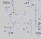
1) I would remove the active load M14 and cascode M9 with a bipolar transistor.
A simple resistor voltage divider to bias the cascode should suffice.
2) Remove the exrta pair of fets in the differential.
3) Use a bipolar current source for the differential (makes it easier to adjust the current). Much like the VAS.
4) Replace R36 with a trim pot for easy adjustment.
This should be a good start.
Jam
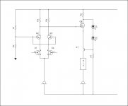
Don't use DN2540, use a bipolar and connect the base to a voltage source at half rail voltage.
Use at drain of mosfet (above)
Use at drain of mosfet (above)
Last edited:
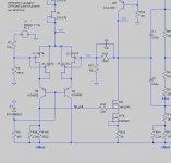
Another attempt below. I think I've got it right this time. (The resistor ladder turned out to be surprisingly finicky.)Hi Jeff,
1) I would remove the active load M14 and cascode M9 with a bipolar transistor.
A simple resistor voltage divider to bias the cascode should suffice.
Hey, I saw Nelson do it in the J2 so thought it must be a good idea. 😉 (Then again, I guess the J2 has no VAS...).2) Remove the exrta pair of fets in the differential.
I originally had it this way, but the bottom CCS transistor needs a heatsink whereas the JFETs share the dissipation.3) Use a bipolar current source for the differential (makes it easier to adjust the current). Much like the VAS.
4) Replace R36 with a trim pot for easy adjustment.
R110 is the trimpot. I've just always shown them as resistors with a label in spice.
Thanks again for all the feedback!
Cheers,
Jeff.
Attachments
Cascode should be npn not pnp, and obviously flip it around so the emitter is connected to drain of mosfet.
Set voltage divider to about half rail voltage to start with.
Set voltage divider to about half rail voltage to start with.
Last edited:
I originally had it this way, but the bottom CCS transistor needs a heatsink whereas the JFETs share the dissipation.
Borrow ZM's opto CC in the Bablefish J2 I linked earlier
Borrow ZM's opto CC in the Bablefish J2 I linked earlier
That's for the output device CCS; Jam and I were discussing the LTP CCS. (Or were you suggesting using an optocoupler there?)
@RNMarsh, THD 0.0005% @ 1W, 0.08% @ 120W. Not built yet, so those are according to SPICE.
@2pico, no, I can't make it work. A fixed bias off the rail doesn't work because the VAS swings from more-or-less rail to rail. I've tried bootstrapping the bias off the VAS output, but it gets squirrelly. I might give it another go tomorrow....
@2pico, no, I can't make it work. A fixed bias off the rail doesn't work because the VAS swings from more-or-less rail to rail. I've tried bootstrapping the bias off the VAS output, but it gets squirrelly. I might give it another go tomorrow....
@RNMarsh, THD 0.0005% @ 1W, 0.08% @ 120W. Not built yet, so those are according to SPICE.
@2pico, no, I can't make it work. A fixed bias off the rail doesn't work because the VAS swings from more-or-less rail to rail. I've tried bootstrapping the bias off the VAS output, but it gets squirrelly. I might give it another go tomorrow....
In that case, just use a voltage source from ltspice, just the voltage symbol and attach to base of transistor, ground the other end and just keep changing values till it starts working correctly, once you know the voltage, then substitute in some circuitry to take the place of the ltspice voltage source.
It should be straight forward. You could post what you have, it might be a silly mistake, I make them all the time.
- Home
- Amplifiers
- Pass Labs
- JamJar: an HPA-1-inspired power amp