Closer to what you suggested?
The basic circuit is that the ref goes to Q1 base, so the LPT can compare that ref with (a sample of) Vout and correct when necessary. In this schematic, what is done with the zener voltage? Nothing, so it can't worjk as a ref.
There is no reference to Q1, it's just Vout.
Take the original circuit and look at how the zener is fed through some R from Vin. Only ONE change: take that feed and move that to Vin. Don't think too much behind it. Just ONE change of a resistor from Vin to Vout, so all the current through that resistor that goes down to ultimately the zener now comes from Vin instead of from Vout.
BTW, normally such a regulator should start up, but there might be a chance it will not. So try it out before modding all your 24 regulators ;-)
BTW2: the resistor-zener string will now be fed from a lower voltage. So you should lower that top resistor so the zener current stays about the same (not critical).
Jan
Attachments
Last edited:
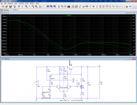
The circuit is pretty much optimal, meaning little room for improvement with this topology.Are there any values we could change in the three transistor regulator to improve results? As it is now we get 77dB @ 10Hz
You can tweak some values, to marginally increase the loop gain, but you are going to scrape a few dB's at most.
The floor is dictated by the Early effect in the transistors, thus you could in principle improve matters by chosing transistors having a higher Vaf, problem: this parameter is not specified in the DS, and the value given in the spice model is generally fanciful and unreliable.
It is also possible to compensate this effect with a resistor, R11 in this case, but a series cap also needs to be added, to compensate for phase-shifts.
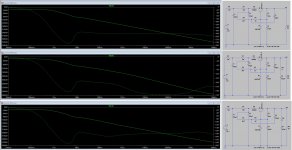
The result looks wonderful: 100dB PSRR @ 10Hz, but it is too good to be true: this is just a simulation, and the reality will be somewhat duller.
You can realistically expect a 20dB improvement, but you will need to make R11 adjustable, because real transistors will not behave in this way.
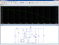
A less glamorous but more reliable solution is to add a passive filter in front of the regulator, like for the Luxman:
Attachments
Things seem to have got clearer and simpler, with just two major options, changing minor details on one or the other. That is very good and what I wished to get by coming here.
The two shown share the same input R/C filter, and the resulting sim curves are both very good.
The simpler regulator, based on the original supply, looks like the best choice in quantity of parts, almost half. Which would mean a simpler pcb that I could even add on the power amp pcb itself, which is a very good thing.
Still pending is the question of the additional voltage I need for the regulator's drop off an for the +/-10v more I need for the low current stages. Using doublers I would have 1.6W per transistor to dissipate, which I think is a bit high. Certainly would need a small HS.
Maybe adding a small transformer to the main one is wiser.
Attachments
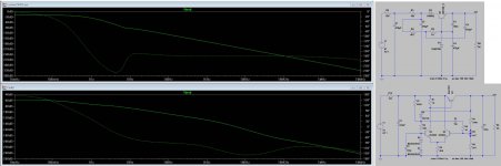
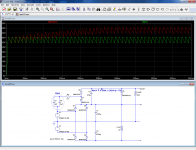
The top one doesn't have an output cap. That has a major impact on loop gain. There will in practice always be an output cap.
To make the sim more accurate, use an output cap with a small series R equivalent to the ESR of the cap you plan to use. Then check again for stability.
Jan
To make the sim more accurate, use an output cap with a small series R equivalent to the ESR of the cap you plan to use. Then check again for stability.
Jan
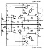
Oh, yes.https://www.diyaudio.com/forums/att...lm317-voltages-goldmund_mimesis_schematic-jpg
I think you are mis-reading it. The "40V" is AC.
"Mindfullness is my second self" 🙂
I mentioned this issue, and provided a low-dissipation solution for boosted rails:Still pending is the question of the additional voltage I need for the regulator's drop off an for the +/-10v more I need for the low current stages. Using doublers I would have 1.6W per transistor to dissipate, which I think is a bit high. Certainly would need a small HS.
Of course, you need to delete the filter option (D5, R1, C3) and duplicate the same circuit for the - rail.
The dissipation will be limited to the excess current wasted in the zener, say 30mA x 12V = 360mW very worst case, meaning you can use a 400mW type safely.
This scheme does need a poly type cap (mylar), but they are small and reliable nowadays, so one 10µF/100V or two 4.7µF/100V should do the job in a quiet and cool manner.
You can tailor the cap size to the actual current required (with some margins, of course)
Nice idea, unfortunately the Early effect affects all the transistors, including the ballast, and the symmetry between Q2 and Q3 does a lot to remove first order effects from the LTP.
The observation that the open-loop compensation works with the LTP's tail confirms this fact.
You cannot filter Q3, for obvious reasons, and if you filter Q2 alone, it is going to make things worse because the first order effect will not be compensated anymore.
One could split R2 to insert a filter to Vin there, but honestly I have no idea how it would fare with the reference and feedback voltages. Could end up much worse.
I would need to sim it, or spend a night having it solved as a background task.
Anyway, the Va of the ballast transistor would remain uncompensated, and it would probably dominate (also to be checked).
There could be another way to find a solution, one never knows until such a solution is found, and I will certainly continue searching, and I encourage you and others to do the same: the content of many brains is always going to prevail, and with the interweb, we can share our findings instantly.
What a wonderful world!
Edit:
I have answered a non-existent post, but the remarks are still valid, thus I will not delete this message
Last edited:
The top one doesn't have an output cap. That has a major impact on loop gain. There will in practice always be an output cap.
To make the sim more accurate, use an output cap with a small series R equivalent to the ESR of the cap you plan to use. Then check again for stability.
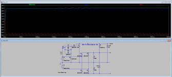
Interestingly enough, the only thing that visibly changed by adding the output cap was the phase curve.
I did add a series resistor to the output cap. I guess that R value would be correct for the cap ESR.
Elvee, can you upload the asc file for the boosted DC lines?
Perhaps I should sim the whole supply, or even add the boosted regulated parts to the amp simulation.
Attachments
Interestingly enough, the only thing that visibly changed by adding the output cap was the phase curve.
Of course. The cap is in parallel with the low Zout of the reg so the output wouldn't change perceptible in magnitude. But it's the phase versus magnitude that determines the stability.
I think these things can be better appreciated when you look at the open loop transfer of the regulator, not the closed loop. You can also do a .tran to see if there are no obvious instabilities.
Jan
With modern types, it is more likely to be something like 0.25 ohm, but with a single transistor, it would be difficult to have instabilities.I did add a series resistor to the output cap. I guess that R value would be correct for the cap ESR.
Without the zener, interesting things could happen: with the numerous capacitors around providing multiple feedback, the response could be quirky, but as soon as the zener conducts, it will kill any resonance.
Here it is, annotated with design information:Elvee, can you upload the asc file for the boosted DC lines?
Attachments
OK, this is an alternative wiring for a doubler as applied by Nelson Pass on his A75 amplifier.
I did retain the D9 zener, but moved all the diodes and caps following what Pass did.
Some questions to understand this simulation, which I never did:
1) Why don't we get smooth DC at the outputs?
2) Why connecting the doubler from main high current bridge instead of directly to the AC output?
3) Why don't we get double the voltage at the boosted output? Shouldn't it be +/-100 VDC?
Attachments
My question over the power amp low current supplies seems to be almost settled for me. And the questions arising seem to be quite minor.
Now I will open another thread to choose a regulated power supply to be used on some RIAA preamps I will be building.
My first idea had been the superregulator, but it has its quirks. So I am considering other options.
I got quite excited when I saw your NoNoiser regulator and its comparison with Jung/Didden specs.
So this is what I plan to propose on that thread: a direct comparison.
One thing I will have is real LTSpice sims comparing several superregulators around.
The next thing, which I don't know if it's possible, is to do actual measurements of the resulting DeNoise and NoNoise regulators.
I already have some super-regulators comparison curves carried on by Linear Audio which I don't know if I can upload to the forum. Will certainly need authorization from Jan Didden to do so.
My first idea had been the superregulator, but it has its quirks.
[]
I already have some super-regulators comparison curves carried on by Linear Audio which I don't know if I can upload to the forum. Will certainly need authorization from Jan Didden to do so.
Carl what quirks are that?
And yes no problem uploading those measurements. Are those the ones by Jack Walton? Most are available already here: https://linearaudio.net/downloads .
But you need to scroll down almost to the end.
Jan
Jan,
Probably no quirks at all. My exaggeration, as they were my first choice in the regulators I plan to use.
The problems that happened in the past have been dealt with by Walt and you, and it's probably the most popular high-grade regulator around.
You do have to follow the recommendations stated by the designers, and maybe that's what I called "quirks". It's not like some other regulators that were less sensitive in that area. But it's the price to pay to have a better regulator.
I believe the measurements I refer to are Walton's. If I'm allowed to upload them on the thread they would be easier to refer to.
Why did you vandalize the circuit in this way? You rendered it non-functional and added useless components.I did retain the D9 zener, but moved all the diodes and caps following what Pass did.
If you tried to fix this "problem", I also provided a variant addressing that:
You wanted the boosted rail to track the main V+, and that's exactly what this variant does (ripple included, obviously).1) Why don't we get smooth DC at the outputs?
You cannot have one behavior and its opposite at the same time in the same circuit: you will have to make a choice.
Here is the non-tracking, smooth version again:
To reference it to the main V+, to avoid this:2) Why connecting the doubler from main high current bridge instead of directly to the AC output?
3) Why don't we get double the voltage at the boosted output? Shouldn't it be +/-100 VDC?
Attachments
No, you got it all wrong.
I didn't vandalize your circuit. That would be a lack of respect, and that's the last thing I wished to do.
What I did was sim the Pass A75 regulator and asked why you had connected the booster parts in a different way than what Nelson Pass had done it?
You can see that I named the asc file that way too.
You wanted the boosted rail to track the main V+, and that's exactly what this variant does (ripple included, obviously).
What I thought to boost was not the main V+ rail, but the AC feeding the large current bridge. Then smooth it, then adding the regulator.
You seem to be proposing a different approach, which I don't quite understand, with a zener diode. Can you explain that?
It seems that it starts as double, or it seems the zener is limiting voltage the booster can get to. Am I right?
My purpose is to get this doubler not to affect anything with additional noise, for instance. On Pass A75 supply the extra voltage is dissipated on the regulator's output transistor, even if voltages were lower.
As I said previously, the circuit is a capacitive supply*, which is loosely based on the doubler topology, but with the front cap small enough to act as a (lossless) ballast.
Without the zener, the final voltage would reach 3*V+
*Search this expression
Without the zener, the final voltage would reach 3*V+
*Search this expression
OK, I will try that capacitive supply for the low current booster.
I imagine there's no way to, but can we trim the regulated voltage output on the single transistor regulator?
That would certainly be a good reason to go back to the 3-transistor regulator, because we have a trimpot there.
I imagine there's no way to, but can we trim the regulated voltage output on the single transistor regulator?
That would certainly be a good reason to go back to the 3-transistor regulator, because we have a trimpot there.
- Home
- Amplifiers
- Power Supplies
- Using the LM317 with higher voltages